This thread has been locked.

If you have a related question, please click the "Ask a related question" button in the top right corner. The newly created question will be automatically linked to this question.

TS5A3160: TS5A3160 damage (or no function) question + Would it be fine if I power TS5A3160 by 5V to V+ but supply IN (pin6) with 3.3V?

Part Number: TS5A3160
Other Parts Discussed in Thread: SN74LVC1G17

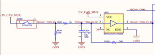
Hi, I'm currently using TS5A3160 to switch 120-ohm termination on and off for CAN FD buses in our ESC (electronic speed controller) design.

This board is designed as an ESC (electronic speed controller) for the BLDC motor.

There's an external dip switch to toggle 3.3V on/off to feed 3.3V into TS5A3160 IN (pin 6) pin for switching.

Currently, the TS5A3160 is powered by 5V on V+.

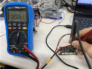
I noticed a weird phenomenon during testing - after my motor control test running the BLDC motor, sometimes I cannot measure the terminating resistance across CAN_H and CAN_L. Only if I just power on the board and toggle the dip switch on, I can measure the 120ohm resistance across COM-NO (CAN_H/CAN_L).  But TS5A3160 is only toggled via a mechanical dip switch. Is the resistance possible to measure with a multimeter?

Just in case, I also tried to capture if there's any voltage spike occurring on 3.3V/5V during motor operation causing the resistance cannot be measured phenomenon yet I couldn't find any anomaly on the waveform with an oscilloscope so far.

1) The first question is - 

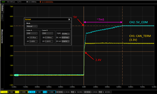
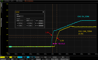
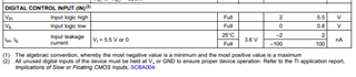
I'm wondering if TS5A3160 can detect logic high correctly in this setup? I checked Vih in the datasheet - when V+ is 5V, a minimum 2.4V should be present for it to be logic high. I assumed it should be fine detecting logic high. PS. Currently, there's no debounce circuit on the dip switch output signal but I'm thinking to add one. (The overshoot captured on CAN_TERM which is connected to pin 6 IN is 4V maximum when the dip switch is toggled but I want to eliminate the mechanical bounce.) 

3) Is there any sequence requirement for the IN (pin 6) to V+? In the current design for this prototype, during my test, there's a possibility that when the USB is plugged into the ESC, the external USB 5V would convert to 3.3V and supply to pin IN. Only afterif I turn on the 24V from the power supply, the on-board 5V then will be converted from 10V on the board with an LDO.

4) The third question is - I have 2 boards, the TS5A3160 on them are either damaged or not functioning. (Most likely are damaged due to the chip is draining excessive current drained on 5V - somewhere around 54mA with calculation because 5V is converted by an LDO from 10V, 10V is converted by a switching regulator from 24V), after removing TS5A3160, the total current consumption is back to the same amount as the board that TS5A3160 is functional. 

I'm worried this could be related to the mux chip damage (or not functioning properly) What are the possibilities that may have caused this failure- 1) chip damage? 2) cannot measure resistance after motor running but when first powering up I can measure the resistance across COM-NO (CAN_H to CAN_L) normally?

Would you kindly provide some insight into this potential TS5A3160 chip damage (or not functioning) issue and review the circuit around the TS5A3160 as attached? (There are 2 other muxes in the schematic SN74LVC1G3157DSFR for other PWM switching purposes. But currently, these 2 muxes are not populated and this function is not used, shown as DNP, please ignore that part of the section.)

And if my above description is unclear to you, please let me know where to address more.

TS5A3160.pdf

  • Add to Phrasebook
    • No word lists for English → Traditional Chinese...
    • Create a new word list...
  • Copy
  • Add to Phrasebook
    • No word lists for English → Traditional Chinese...
    • Create a new word list...
  • Copy
  • Add to Phrasebook
    • No word lists for English → Traditional Chinese...
    • Create a new word list...
  • Copy
  • Add to Phrasebook
    • No word lists for English → Traditional Chinese...
    • Create a new word list...
  • Copy
  • Add to Phrasebook
    • No word lists for English → Traditional Chinese...
    • Create a new word list...
  • Copy
  • Add to Phrasebook
    • No word lists for English → Traditional Chinese...
    • Create a new word list...
  • Copy
  • Add to Phrasebook
    • No word lists for English → Traditional Chinese...
    • Create a new word list...
  • Copy
  • Add to Phrasebook
    • No word lists for English → Traditional Chinese...
    • Create a new word list...
  • Copy
  • Add to Phrasebook
    • No word lists for English → Traditional Chinese...
    • Create a new word list...
  • Copy
  • Add to Phrasebook
    • No word lists for English → Traditional Chinese...
    • Create a new word list...
  • Copy
  • Add to Phrasebook
    • No word lists for English → Traditional Chinese...
    • Create a new word list...
  • Copy
  • Add to Phrasebook
    • No word lists for English → Traditional Chinese...
    • Create a new word list...
  • Copy
  • Add to Phrasebook
    • No word lists for English → Traditional Chinese...
    • Create a new word list...
  • Copy
  • Add to Phrasebook
    • No word lists for English → Traditional Chinese...
    • Create a new word list...
  • Copy
  • Hey Chieh Wei,

    So for the questions presented


    Is the resistance possible to measure with a multimeter?

    I'm a little unclear here. Are you trying to measure the resistance across the TS5A3160? Using a multimeter won't work here. You'll need to source some current as shown in the datasheet setup in figure 13.


    1)

    I'm wondering if TS5A3160 can detect logic high correctly in this setup?

    Is the only concern here just from the debounce? Looks like the VIH/VIL levels are understood (2.4V/0.8V) properly and it's just more of a concern if the debouncing will be an issue. It may be an issue but the over voltage to 4V won't. The only issue will be if the debouncing sending the signal between the VIH/VIL levels. Here there may be some oscillation and/or shootthrough current momentarily. Some times this transient won't be an issue but adding something to mitigate the debounce is a good idea.

    3) (there wasn't a number 2)

    Is there any sequence requirement for the IN (pin 6) to V+?

    The device doesn't have fail-safe logic so it would be recommended to power up the V+ first and then the input signal. Fail-safe logic will protect from backpowering and any bootup issues. Here's a video on this 2.11 TI Precision Labs - Switches and muxes: What is fail-safe logic?.

    4) 
    Could you provide more information on what the issue being seen is? My understanding is that the current on the VCC is higher than anticipated. 54mA wouldn't damage the device however but it is higher than expected. If it functioning properly still?
    Addiiontally what does the input tot he CAN_TERM look like? I believe it's ramping up to 3.3V but how fast is this level? The slower the edge on the control pin the longer you'll remain in the region between VIH/VIL where there will be more shoot through current and this could be potentially part of what is being seen.

    Thanks,
    Rami

  • Hi Rami,

    Thanks for your reply.

    I'm a little unclear here. Are you trying to measure the resistance across the TS5A3160? Using a multimeter won't work here. You'll need to source some current as shown in the datasheet setup in figure 13.

    Yes, I was trying to measure the 120ohm resistance across the CAN_H/CAN_L passing through TS5A3160 when IN is in the logic high state, namely the board is in operation. I was able to get the value 120ohm showing at the initial powering up the board (and TS5A3160 device) if the dip switch is toggled. After performing some motor control movement, I couldn't get the value from a True RMS multimeter anymore. So I was concerned. But apparently, it wasn't the right way to measure the resistance across COM-NO poles based on your reply.

    Is the only concern here just from the debounce? Looks like the VIH/VIL levels are understood (2.4V/0.8V) properly and it's just more of a concern if the debouncing will be an issue. It may be an issue but the over voltage to 4V won't. The only issue will be if the debouncing sending the signal between the VIH/VIL levels. Here there may be some oscillation and/or shootthrough current momentarily. Some times this transient won't be an issue but adding something to mitigate the debounce is a good idea.
    The device doesn't have fail-safe logic so it would be recommended to power up the V+ first and then the input signal. Fail-safe logic will protect from backpowering and any bootup issues. Here's a video on this 2.11 TI Precision Labs - Switches and muxes: What is fail-safe logic?.

    The concern was if it is OK for TS5A3160 to operate when V+ = 5V with IN = 3.3V input because the 2x TS5A3160 devices are not functioning or damaged on our board, and if the logic level is not the cause then I can rule it out. I was worried that if the device is designed with accepting this V+ = 5V, IN=3.3V configuration. From the way it sounds, it is acceptable? Then I guess probably have 2 options? 

    1) change the control pin IN to change to another source, e.g. onboard control signal or 5V;  and then add debounce and rc delay, so the "CAN_TERM can be powered up before 5V_COM is present" scenario can be avoided completely.

    2) change to another part (if there's one pin-to-pin compatible) with fail-safe logic (not the most preferable way because we've already purchased this part for our first production even though it's just a few hundred pieces and the date is near, but if there's no better option).

    Could you provide more information on what the issue being seen is? My understanding is that the current on the VCC is higher than anticipated. 54mA wouldn't damage the device however but it is higher than expected. If it functioning properly still?

    On those 2 particular boards, the device TS5A3160 seems to be not functioning anymore (Because over CAN bus, I cannot detect these 2 particular boards if set them as the last node respectively - due to termination is not properly set. While on all the other boards were detecting fine). And in the very beginning, the TS5A3160 devices on these 2 boards 'were' functioning.

    Addiiontally what does the input tot he CAN_TERM look like? I believe it's ramping up to 3.3V but how fast is this level? The slower the edge on the control pin the longer you'll remain in the region between VIH/VIL where there will be more shoot through current and this could be potentially part of what is being seen.

    Attaching scope shots here measuring 5V_COM to CAN_TERM (3.3V feeds into TS5A3160 <IN> pin with 100ohm pull-down)

    The first picture is showing it takes roughly 7ms for the 5V LDO to turn on 5V after powering up and reaching the steady-state. It seems the LDO is behaving this way on the board even without any device at the back of the power rail (there's  another 5V rail using the LDO.)

    In the second picture, I measured the waveform when dip switch is toggled on and then power up the board. I put the cursor around 1.8V level for 5V_COM, and 1.5V (Vih) for 1.8V to work, the switch-on time for the mux reaches minimum 1.8V level, and the control <IN> pin reaches minimum 1.5V level (for 1.8V Vih) is roughly 58uS. It seems the 5V is still ramping up earlier than I'm not sure if it is how do you see when the mux starts up though.)

    Please kindly let me know what you think.

    Thanks,

    Bertram

    • Add to Phrasebook
      • No word lists for English → Traditional Chinese...
      • Create a new word list...
    • Copy
    • Add to Phrasebook
      • No word lists for English → Traditional Chinese...
      • Create a new word list...
    • Copy
    • Add to Phrasebook
      • No word lists for English → Traditional Chinese...
      • Create a new word list...
    • Copy
    • Add to Phrasebook
      • No word lists for English → Traditional Chinese...
      • Create a new word list...
    • Copy
    • Add to Phrasebook
      • No word lists for English → Traditional Chinese...
      • Create a new word list...
    • Copy
    • Add to Phrasebook
      • No word lists for English → Traditional Chinese...
      • Create a new word list...
    • Copy
    • Add to Phrasebook
      • No word lists for English → Traditional Chinese...
      • Create a new word list...
    • Copy
    • Add to Phrasebook
      • No word lists for English → Traditional Chinese...
      • Create a new word list...
    • Copy
  • So for the first point,

    From the way it sounds, it is acceptable? Then I guess probably have 2 options?

    Yes this is acceptable to have V+ = 5V and IN = 3.3V (see below from datasheet)

    That being said, typically we recommend that you switch at the rails (0V for Low and Vcc for High). This just reduced extra current consumption. 

    The sequencing from the second pic seems fine. The power gets to spec before the voltage input at V+ begins ramping up. My concern was more with how long it takes to ramp up the logic control. The longer it stays within the voltages between VIH/VIL the more shoot through current. 

    What exactly are you seeing that causes you to define the devices as 'not functioning'? (Is it not switching between channels, does it have physical damage, are you seeing excessive current draw through VCC, are no signals passing through the switch, etc.?)
    And what are the characteristics of the CAN voltages that are going through the switch?

    Thanks,
    Rami

  • What exactly are you seeing that causes you to define the devices as 'not functioning'? (Is it not switching between channels, does it have physical damage, are you seeing excessive current draw through VCC, are no signals passing through the switch, etc.?)
    And what are the characteristics of the CAN voltages that are going through the switch?

    Hi Rami,

    Sorry for the messy information. To summarize, I have 36 boards in total. 2 boards I'm seeing abnormal behaviour related to the mux compared with the other 34 boards.

    I don't see any physical damage. Both with excessive current draw through VCC. The excessive current draw through VCC would be gone if I remove mux. One in particular caused CAN voltage to be pulled low.

    #1 board, mux is not functioning, excessive current (~60mA more than the other 34 'good' boards) was drawn on 5V rail. CAN voltage is pulled to 1.5V always disregarding whether I toggle the dip switch or not. When removing the mux, the current drawn on 5V become normalized compared with the other 34 boards. When I remove the 120-ohm termination. It seems CAN_H was pulled low abnormally to 1.5V while CAN_L still stays at 2.5V when idle (no CAN communication). There was no CAN communication. When I removed the mux, the CAN_H voltage also got back to 2.5V. 

    #2 board, the mux is still "functioning" as when 120-ohm termination was removed I could still see the NO output being switched on or off when the dip switch was toggled. But the power consumption was abnormal on the 5V rail compared with the other 34 boards. Higher current drawn from mux on 5V rail (~16mA more than other 34 'functioning' boards).  On the good boards, the mux consumes very little less than 1mA.

    Thanks,

    Bertram

    • Add to Phrasebook
      • No word lists for English → Traditional Chinese...
      • Create a new word list...
    • Copy
    • Add to Phrasebook
      • No word lists for English → Traditional Chinese...
      • Create a new word list...
    • Copy
    • Add to Phrasebook
      • No word lists for English → Traditional Chinese...
      • Create a new word list...
    • Copy
    • Add to Phrasebook
      • No word lists for English → Traditional Chinese...
      • Create a new word list...
    • Copy
    • Add to Phrasebook
      • No word lists for English → Traditional Chinese...
      • Create a new word list...
    • Copy
    • Add to Phrasebook
      • No word lists for English → Traditional Chinese...
      • Create a new word list...
    • Copy
    • Add to Phrasebook
      • No word lists for English → Traditional Chinese...
      • Create a new word list...
    • Copy
    • Add to Phrasebook
      • No word lists for English → Traditional Chinese...
      • Create a new word list...
    • Copy
    • Add to Phrasebook
      • No word lists for English → Traditional Chinese...
      • Create a new word list...
    • Copy
    • Add to Phrasebook
      • No word lists for English → Traditional Chinese...
      • Create a new word list...
    • Copy
    • Add to Phrasebook
      • No word lists for English → Traditional Chinese...
      • Create a new word list...
    • Copy
    • Add to Phrasebook
      • No word lists for English → Traditional Chinese...
      • Create a new word list...
    • Copy
    • Add to Phrasebook
      • No word lists for English → Traditional Chinese...
      • Create a new word list...
    • Copy
    • Add to Phrasebook
      • No word lists for English → Traditional Chinese...
      • Create a new word list...
    • Copy
    • Add to Phrasebook
      • No word lists for English → Traditional Chinese...
      • Create a new word list...
    • Copy
    • Add to Phrasebook
      • No word lists for English → Traditional Chinese...
      • Create a new word list...
    • Copy
    • Add to Phrasebook
      • No word lists for English → Traditional Chinese...
      • Create a new word list...
    • Copy
  • Hi Chieh,

    We are on Holiday in Dallas today and we are returning tomorrow and will return to answer your follow-up.

    Best,

    Parker

  • Hey Bertram,

    I'm not certain why this phenomena is happening yet but could you do you some functional tests here to try and pinpoint what is happening? 
    Could you do a simple ABA swap? Just replace the non functional device with a known working one and see if the problem is still there. Then replace it back with the damaged one and see if the problem persists. Looking to see here if this is the IC itself or some system level issue on those specific boards. Seems that you have removed the device and tested without the device but I don't believe you have replaced a functional device in its place; or atleast you haven't shared if you have.

    Also could I get more information on this current? Is it sustain current? As in does the 54mA or 16mA stay constant the entire time or does get lower over time or does it spike at a certain interval?

    I do have a system level question here, however. I haven't seen the 120ohm termination being connected and disconnect on a CAN bus. My understanding on CAN bus was that the termination was a requirement. What's the purpose of doing this, if you don't mind me asking?

    Thanks,
    Rami

  • I'm not certain why this phenomena is happening yet but could you do you some functional tests here to try and pinpoint what is happening? 
    Could you do a simple ABA swap? Just replace the non functional device with a known working one and see if the problem is still there. Then replace it back with the damaged one and see if the problem persists. Looking to see here if this is the IC itself or some system level issue on those specific boards. Seems that you have removed the device and tested without the device but I don't believe you have replaced a functional device in its place; or atleast you haven't shared if you have.

    I'm sorry for late reply. Because was busy working on other issues.

    The #1 board with dysfunctional chip is unfortunately damaged in other test. The mux on the board is most likely also damaged because after sending the last message while performing other some measurement, there was a direct short on the CAN bus to 24V. So it is no longer usable. On the #2 showing some weird current, after performing ABA swap with another known good board, the current consumption has become normalized. The weird current consumption is following the multiplexer and is occurring on the known good board #3. 

    Also could I get more information on this current? Is it sustain current? As in does the 54mA or 16mA stay constant the entire time or does get lower over time or does it spike at a certain interval?

    It was sustain-current on #2. But after I performed ABA swapped, on the known good board #3 with the potential defect mux, I'm seeing current jumping up and down. And after a few minutes, the current seems to become lower. I cannot see if there's any pattern or certain internal on the pattern. 

    I do have a system level question here, however. I haven't seen the 120ohm termination being connected and disconnect on a CAN bus. My understanding on CAN bus was that the termination was a requirement. What's the purpose of doing this, if you don't mind me asking?

    The reason to have this multiplexer switching 120ohm on and off is that we use the same boards in our robot and we use the multiplexer to only switch on the board at the last node. We were using pin headers to manually place the jumper socket. But during development, we've encountered several times the pin header connector being damaged during assembly (the entire pad gets peeled off) or jumper socket got loose and fell off. Then found a reference design from another vendor using their multiplexer to switch the 120ohm termination, therefore we chose to implement a similar concept but switch to TI's solution (because I trust in TI's analog multiplexer chip quality).

    One thing I'm suspecting is that for #1 and #2 boards, I was toggling the dip switch in hot. Meaning with the mechanical signal bouncing might be present while I was switching the dip switch while power is supplied. Although I'm not sure if it would potentially damage the CMOS input, according to your "TI application report <Implications of Slow or Floating CMOS Inputs, SCBA004>, from 0.8V to 2V duration is applied to the input for a prolonged period of time, might cause some damage to the internal circuit

    Right now I've added another RC circuit with SN74LVC1G17DCKR (another TI part) Schmitt-trigger buffer IC as debounce circuit. Also, change pin 6 (IN) of TS5A3160 to 5V input. I still need to tune the RC value on SN74LVC1G17DCKR input, if there's any comment or suggestion on the Schmitt-trigger buffer selection I would be very grateful. 

    V3 MUX Circuit.pdf

    • Add to Phrasebook
      • No word lists for English → Traditional Chinese...
      • Create a new word list...
    • Copy
    • Add to Phrasebook
      • No word lists for English → Traditional Chinese...
      • Create a new word list...
    • Copy
    • Add to Phrasebook
      • No word lists for English → Traditional Chinese...
      • Create a new word list...
    • Copy
    • Add to Phrasebook
      • No word lists for English → Traditional Chinese...
      • Create a new word list...
    • Copy
  • Hey Chieh,

    Slow inputs could certainly cause shoot through current which would increase total current consumption. I wouldn't expect this to damage the device though if the source is just some bouncing from the dip switch; depending on how long that takes. There may be some inrush from the hot switch. I would probe to see how the inrush voltage and current look when hot switching to see what the input looks like as you're doing that and if it violates any specs. However, this all seems as a mute point since you're adding the SN74LVC1G17 schmitt trigerr.   

    With regards to the SN74LVC1G17CKR, this looks like it would be a good fit for the device. With the 5V output of the schmitt trigger being fed into the TS5A3160 (VIH/VIL = 0.8V/2.4V) control pin, the device will be able to be controlled properly and reduce any bouncing that may be giving issues.

    I'm going to loop in the product line that is responsible for the 1G17 device to see if there are any extra comments or recommendations here just to make sure we've covered all our bases.


    Thanks,
    Rami

  • Hi Chieh,

    The debounce circuit looks good to me -- rising edge has about 2ms delay and the falling edge has about 20ms, which is exactly what I would recommend.

    One very minor area of concern might be overshoot - since the LVC1G17 has a very strong output driver and you're probably connecting these two circuits with a very short trace, there may be excessive ringing. One thing you can do to avoid issues is to add a series 0 ohm resistor at the output of the LVC1G17 (pin Y), which can be swapped out for a larger resistor later if excessive ringing is found to be a problem.