This thread has been locked.

If you have a related question, please click the "Ask a related question" button in the top right corner. The newly created question will be automatically linked to this question.

PMP8740: Opto isolated feedback

Part Number: PMP8740
Other Parts Discussed in Thread: UCC28950, PMP8606, PMP10110, , PMP7246

Hi TI expert

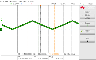
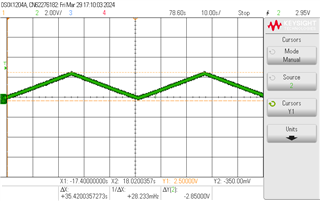
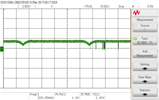
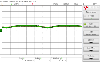
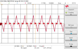
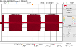
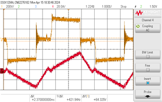
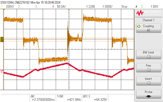
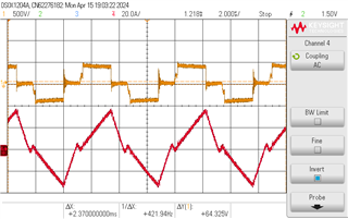
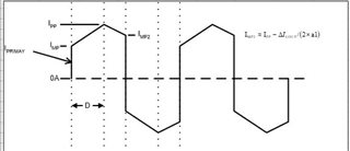
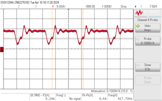
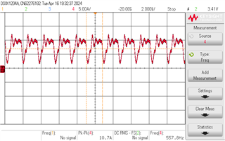
I am using UCC28950 PSFB IC for EV charger proto

Input is 380V DC to 425V DC, Power is 3500 Watts

I want to evaluate PSFB controller IC alone first and would like to know procedure to calculate for OPTO feedback system which i followed PMP8606

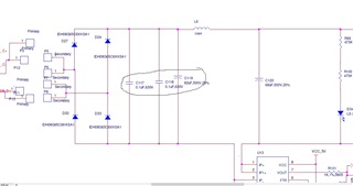
Attached is the schematics and EXcel sheet i used 

Thank you

SLUC222D_3_5kw.xlsPSFB.pdf

  • Hi Venkatesh,

    You can use the feedback section from PMP8740 and add the optocoupler, similarly to the design PMP10110 (https://www.ti.com/tool/PMP10110).

    In PMP8740, D1 and D3 are pulling down pin 2 of U2, while R2 is the pull-up resistor.

    It is possible to do it as shown in PMP10110, where D10 and D11 are equivalent to the diodes in PMP8740, while here the pull-up resistor is R37 (which defines also the current through the emitter diode). Now, if you use PMP10110 feedback circuitry, you can connect pin 3 of U4 to ground, and pin 4 of U4 to EA+ pin (pin 2) of the UCC28950.

    Please let mw know if that makes sense.

    Regards,

    Roberto

  • Hi Roberto,

    Thanks i am doing this, let me clarify one thing instead of EA+ pin, can i use EA- pin as followed in the PMP8606

    Attached my updated schematic, kindly confirm its functionality please

  • Hi Roberto,

    Thanks i am doing this, let me clarify one thing instead of EA+ pin, can i use EA- pin as followed in the PMP8606

    Attached my updated schematic, kindly confirm its functionality please

    psfb_updated.pdfopto.pdf

  • Hi Venkatesh,

    Both solutions, of connecting the output of the optocoupler to EA+ (PMP8740) or as in PMP8606 (EA-) are possible, even though, if i have to choose, I prefer my method in PMP8740 :-).

    Anyway, if possible please send me the schematic when you are done connecting the optocoupler to EA- pin. 

    In addition, by analyzing your schematic, just consider that R8 and R46 cannot be selected as zero-Ohm resistors, because otherwise when Q13 and Q14 are switching at certain duty cycle, these small signal MOSEFTs will short those capacitors and you will not get any voltage on C5 and C17.

    Regards,

    Roberto

  • Hi Roberto,

    Thank you, i have changed R8 and R46,as of now i am testing only PSFB board and giving Vref signal through Microcontroller.

    I have calculated set voltage as 2.8V and output voltage sense also 2.8V

    when i am turned on MCU and PSFB controller no pwm output came

    Attached updated schematic of both PSFB & Opto section to EA- section

    Kindly let me know what shall correction to be done

    opto1.pdf4478.psfb_updated.pdf

    Thank you

    venkatesh B

  • Hi roberto,

    could you please update 

    Thank you

    venkatesh B

  • Hi Venkatesh,

    Can you please measure with a meter, or better with a scope, the voltage on R56 (output of optocoupler Vopto) referred to ground? If this voltage is zero, then the controller should generate all PWM signals. If Vopto is in your board> 2.5V, then there will be no PWM.

    Please let me know.

    Regards,

    Roberto

  • HI  Roberto 

    PFA scope data at various points,to test i have given Vref and Iref from 100% duty cycle to 1% duty cycle and captured entire time frame alike in seconds

    U39 Pin 3 to Gnds

    U39 Pin 5 to Gnds

    U39 Pin 1 to Gnds

    U39 Pin 7 to Gnds 

    Across R235

    U17 Pin 1 to 2 

    U17  Pin 4 to 3

    Across R56

    Thank You

    Kindly let me know what changes to be done

  • Hi roberto could you please check and let me know

  • Hi Venkatesh,

    Sorry, yesterday it was holiday in Germany.

    I see here two things:

    1) It looks like R228 has a limit resistance value 10 kOhm; the current through this resistor might be insufficient if the CTR of U17 is lower than 100%. Nevertheless, this should not impact your current measurements. Anyway, please use 4.7 kOhm for R228 to have margin.

    2) When you have some reference on pin 2 or 6 of U39, and at the same time no voltage on net V_SNS nor I-BAT-IST (like in the case Vout and Iout are both zero), the controller U1 should deliver pulses.

    I assume you already activated U1 by providing the net PSFB_EN a 3.3V or 5V, didn't you? If not, please activate the controller this way.

    Also, please check that U39 is supplied and pin 8 has 12V supply.

    Thanks,

    Roberto

  • Hi roberto

    Thank you, i will change to 4.7K and check it

    sorry to disturbed you on holiday

    regards

    venkatesh B

  • Hi Roberto,

    I have removed current section path from feedback section and can able to control voltage from giving Vref signal from MCU

    Then i bypassed voltage section and current control is possible after i kept current section at load side completely

    Now when i loaded with rheostat it is limited to 7A,attached PSFB primary side current,

    what could be reason for not achieving 3KW of Power

    Input is 400V DC

  • Hi Venkatesh,

    When you say:

    1) "I have removed current section path from feedback section", do you mean you removed D3?

    2) "able to control voltage from giving Vref signal from MCU", which voltage?

    3) "I bypassed voltage section", do you mean you removed D57?

    4) "Current control is possible", what current?

    5) "After i kept current section at load side completely", sorry I don't understand this.

    Can you please let me know the answer to my questions? In addition, can you please add the schematic of your power stage?

    Regards,

    Roberto

  • Hi roberto,

    Yes i have removed D3 to validate Voltage section alone,I mean output voltage reached maximum 420V DC by varying PWM_Vref signal from MCU.

    then i removed Voltage section by removing D57 and connected Rheostat load at PSFB output side then giving PWM_Iref gradually from 100% to 10%,output current Increases from 0 to 7A gradually and settled

    Now in this current control alone i want to go till 8A,but 8A,420V getting when input DC is 340V DC,while at input is 400V DC,converter limits its output to 7A and 350V DC only

    Thank you

    venkatesh B

  • Hi Venkatesh,

    OK, everything is clear now, thank you.

    Please consider that when the peak voltage on CS pin of UCC28950 reaches 2V, the converter will start limiting the current, so please check whether you see a current sense voltage > 2V on cathode of D2.

    Additionally, please double check that when you set PWM_IREF to maximum value, the equivalent voltage on pin 5 of U39 is higher than the current sense signal output at maximum power stage output current. Sorry, if you need more precisely analysis and tell you exactly which voltage to check, then I need to have also the power stage schematic.

    Regards,

    Roberto

  • Hi roberto,

    Yes CT is limiting the power , I have replaced the burden resistor to 100 Ohm,2W

    Now i can able to control to 3KW,8A rheostat load

    Thank you for your support

    I will check to incorporate both V & I in same opto as well and kindly give me steps to achieve ZVS/ZCS  since at full load PSFB fet,diodes and Transformer getiing heated up

    Thank you

  • Hi Venkatesh,

    Glad to see you solved this limiting power issue.

    I assume you are using MOSFETs on PSFB primary side and diodes on secondary side, or are you using also sync-FETs?

    If you are using diodes, please be sure to employ SiC diodes.

    If using sync-FETs, for this high Vout voltage application, I suggest to have 4 sync-FETs instead of center tap rectification, because it's reducing the voltage stress.

    Regarding achieving ZVS on primary side, you need to add a shim inductor, because relying only on leakage inductance of the transformer is increasing full load efficiency, but reducing light load and mid-load efficiency.

    Regards,

    Roberto

  • Hi roberto,

    Yes i am using SIC Diodes at secondary side.

    I will add shim Inductor and explore

    Thank you Roberto

    Regards 

    Venkatesh B

  • hi roberto,

    i have added shim inductor of value 10uH.all the four mosfet blown away

    I have replaced with new fets and removed shim inductor completely,At full load,Primary mosfets are reaching 95 deg and still increasing .temperature is the problem now

    I observed that even at full load it operates at DCM mode.i did varying Rdcm value also no response

    What shall i do now?

    thank you

    venkatesh

  • Hi roberto 

    could you please update

    Thank you

    venkatesh

  • Hi Venkatesh,

    I have few questions about the power stage:

    1) According to the excel calc-sheet you attached at the beginning, you selected the primary magnetizing inductance of the transformer = 1.33 mH....can you confirm?

    2) In addition, do you confirm you are using 202 uH as output inductor (it's also mentioned in the excel sheet)?

    3) Are you using heat sinks on all Mosfets?

    Regards,

    Roberto

  • Hi Roberto,

    1.Yes Transformer is 1.33mH

    2.Output side i am using 10uH only

    3.All four Mosfets and output Diodes are Placed in Heatsinks

    Thank you

    venkatesh B

  • Hi Venkatesh,

    May I ask why are you using only 10uH output inductance? With this value the output ripple current will be very high, and the converter will always run in DCM.....

    Thanks,

    Roberto

  • Hi roberto,

    I have checked with voltage and current,

    Output side it is in CCM mode only

    Thats why i have not increased L value

    During this time PSFB Primary side current is followed

    this is in DCM mode

    I hope its clear

    Let me know if any

    Thanks 

    venkatesh

  • Hi Venkatesh,

    Can I ask what is the red line on first screenshot? What is the orange line?

    At which load current are they taken? Can you set the time scale to 1 usec/div?

    In the second screenshot, the red line is the transformer current (primary side winding), right? Can you please set the time scale to 1 usec/div?

    According to this screenshot, you have ~ 30 Apeak on primary side. It's equivalent to 12kW power...it is actually weird, and can be explained only if the output inductor current is very high......can you please double check it?

    Thanks,

    Roberto

  • Hi 

    Orange line is the Output voltage,red line is the output current 

    second one is Transformer Primary current ,all readings taken at full load 420V,8A output ,input is 400V DC

    i will take 1 us/div also

    Thank you

    venkatesh B 

  • OK, thank you. Please let me know when you take the new waveforms.

  • Hi 

    Transformer voltage and transformer current Primary side(PSFB transformer) at 1us/div

    what could be the reason for heating PSFB fets

    Thank you

  • Hi Venkatesh,

    As you can see, the primary current shows very high peak-peak current. That means on leg of the PSFB is working in hard switching (which will generate very high loss), and the other leg will work in soft-switching but both legs will have high HF current content.

    the solution is to use adequate output inductor (I this you need here at least 120 uH or better 150 uH).

    Can you please replace the output inductor with a bigger one?

    Thanks,

    Roberto

  • ok just a minute

  • Hi roberto 

    I have changed output L to 270uH

    Below Transformer V and I waveforms

    still same response i am getting

  • Hi Venkatesh,

    That is really strange. With this inductor you should see a primary current very close to the attached waveform (taken from the UCC28950 excel calc-sheet.

    Please try to understand where is the issue, maybe by taking a screen-shot of the output inductor current...

    Regards,

    Roberto

  • Ok thanks, i will check

  • Dear Roberto,

    How to select RRE resistor which is connected CT secondary side to sense current,from UCC28950 Excel calc sheet,it was not mentioned only RS is given to choose

    I have taken reference from 2KW design of PSFB PMP8740,how 100K comes.

    Kindly advice value to optimize sensing

    Thank you

  • correct me if i wrong,do i take 100 times of RS for RRE resistor

  • Hi roberto

    Attached waveform of Output inductor,

    Can i cjhange Tabset delay,in 600W reference design it is calculated as 30ns,but 346ns is set

    what could be the reason,can i try the same

    Thank you

    venkatesh B

  • Hi Venkatesh,

    I don't know if I already sent you this, but at the following link you can find all calculations (reflecting the UCC28950 Excel Sheet) for a PSFB with UCC28950:

    https://www.ti.com/lit/an/slua560d/slua560d.pdf

    On page 12, formula (91), Rre is calculated to be 100 * Rs, so you are right about this value.

    This is a minimum value. The maximum value should be selected so that the peak of magnetizing current in the CT, times Rre, produces a voltage that has to be lower than the CT diode rating. For example, if the peak magnetizing current is 500 uH, this current, multiplied by Rre should be lower than the diode rating. 500 uH * 100 kOhm makes 50V, which is fine (I believe the diode support up to 200V).

    Regarding the delay time, I usually select them in  the range of 100 nsec, 200 nsec and fine tune it to avoid too much body diode conduction time. You may want to do the same, I guess.

    Thanks,

    Roberto

  • In addition, I didn't find the screenshot of the output inductor current, can you please attach it again?

  • Hi roberto,

    Sorry it missed,

    PFA output inductort current waveform at full load 

    advice me if any improvement required

    Thank you

  • Hi Venkatesh,

    It looks like the converter is unstable, because oscillates at 417 Hz, so first you have to get a stable system, by adjusting the compensation network.

    Further question: can you please take a screenshot with 1 usec/div time scale?

    Thanks,

    Roberto

  • HI roberto 

    we changed compensation network

    Please find output Inductor at DSO i usec/div

    Thank you

    venkatesh

  • Hi Venkatesh,

    I see the converter is still unstable.

    Can you please summarize which loop is active?

    In addition, can you please share what is your load? Is it a constant current load, or constant resistance or even constant voltage load?

    Or maybe you are using a battery as load.....please let me know.

    In addition, I meant if you can share the screenshot of the inductor current, so I expect to be a triangular current + DC pedestal.

    I think you are sharing the output converter current, isn't it?

    Thanks,

    Roberto

  • Hi Roberto,

    Let me clarify one thing PSFB secondary side is Diode bridge rectifier(SiC diodes) and follows CLC filter.

    Attached schematic fyr

    1538.PSFB.pdf

    Thank you

  • Hi Roberto,

    Could you please check

    Thank you 

    venkatesh B

  • Hi Venkatesh,

    I see on secondary side the four SiC diodes D27, D24, D32 and D33 directly connected to C117, C118 and C119. This connection is allowed for LLC converters but not for PSFB. A PSFB converter follows Forward conversion principle, similar to a Buck, but isolated. A Buck converter has after the switch node (the center of both high-side and low-side MOSFETs) an inductor. The inductor is in charge to create an average voltage, equal to the duty cycle times Vin. Here, the equivalent of the Buck switch node, is the cathodes of D27 and D24. If an output capacitor is connected on that diodes, then Vout will not be = Vin * Ns/Np * D, but will be actually Vin * Ns/Np, so unregulated. Can you please double check whether the schematic is correct?

    In addition, you said before that the output inductor (I believe here L6) was 10 uH, but here I see 1 mH....which value is correct?

    Thanks,

    Roberto

  • Hi roberto,

    L6 is output inductor and its updated value is 300uH(calcuted value is 240uH in excel sheet)

    Above schematic is correct only,can i remove output capacitor D27 and check?

    Thanks 

  • Attached Image,can i remove these capacitor C117,C118 & C119 to obey Vout to be  Vin * Ns/Np * D

  • Hi Venkatesh,

    Yes, please, remove C117, C118 and C119, but consider that you will see spikes on D24 and D27. You should consider adding a snubber network (clamping circuit), similarly to UCC28950 EVM or PMP8740.

    Regards,

    Roberto

  • ok i will do that now

  • Hi roberto, now PSFB Fet temperature is reduced,but secondary side diode is heating up

    what could be the reason

    attached secondary side voltage and output inductor current

    Yellow color is Voltage after rectification

    red is output inductor current

    Now Diode is blasted if we run for long run

    Thank you

    venkatesh