- Ask a related questionWhat is a related question?A related question is a question created from another question. When the related question is created, it will be automatically linked to the original question.
We find INA145UA/2K5 ,DC2042 have about 32% failed in FCT, the detail information as below :
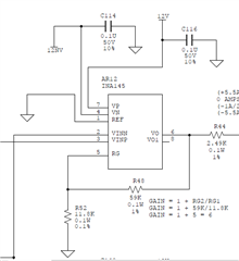
For component level, we did as below: (Designed Gain is as below snapshot, 59K: 1%, 11.8K: 0.1%)
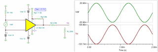
OK Board: pin2~3:-0.0209 VDC, pin6:-0.1259VDC, Gain=6.0239
Failed Board: pin2~3:-0.0208 VDC, pin6:-0.1177 VDC, Gain=5.6586
Pin2/pin3 input about -14.0X VDC.
RG2:59.121K
RG1:11.797K
RG2/RG1=5.0115
Power with +/-12VDC