- Ask a related questionWhat is a related question?A related question is a question created from another question. When the related question is created, it will be automatically linked to the original question.
This thread has been locked.
If you have a related question, please click the "Ask a related question" button in the top right corner. The newly created question will be automatically linked to this question.
Hello Suzuki-san,
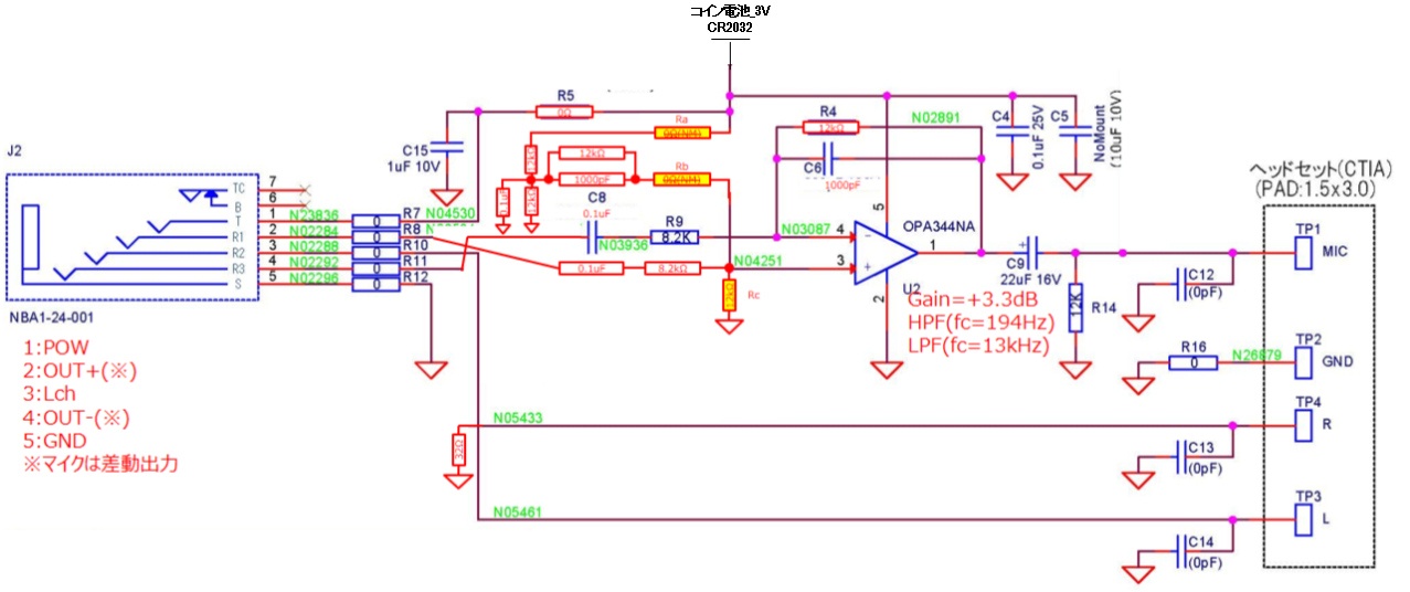
Thank you for reaching out to us. I am copying the schematic into this thread for visibility. I do not see any issues with the schematic as implemented, but you may not see the desired result on your output depending on your input.
Your input common mode would be 0 volts, as well as your output common mode. If you are putting in a sinusoid to out+ and out- you will only see the parts of it that add up to more that 0V. You can fix this by increasing your input common mode to give yourself more headroom on your output.
Also, may I ask if there was a specific reason the OPA344 was chosen? If this is an audio application, we have several other lower noise devices than OPA344, like the OPA375 or the OPA992. I have included a list of parts below with lower noise than OPA344 that can be supplied by 3V.
I noticed in the other thread you stated you were unable to open the .tsc files. I do highly recommend TINA-TI or PSpice for TI to help with these questions as well. TINA TI is fairly simple to use and fairly small as a program, while PSpice for TI includes many spice features and an integrated library of TI parts, so there is no need to download a model from the web. You may build the circuits and simulate them with your inputs and outputs, and most recent models do a good job modeling many features of our devices.
Best,
Jerry
Hello Suzuki-san,
For best dynamic range, U2 output should be 1/2 supply
For lower THD, the input common mode voltage should be far away from input stage crossover.
The circuit below has a Vout at 1.5V and Vcm of 1V . The gain is 4dB.

Dear Jerry-san,
Thank you reply.
> I do not see any issues with the schematic as implemented, but you may not see the desired result on your output depending on your input.
I thank you for your confirmation work.
Also, I will try to manufacture a board with this circuit.
I will look back on your advice if there are any issues with evaluation results.
> Also, may I ask if there was a specific reason the OPA344 was chosen? If this is an audio application, we have several other lower noise devices than OPA344, like the OPA375 or the OPA992. I have included a list of parts below with lower noise than OPA344 that can be supplied by 3V.
I can't judge because test conditions are different.
Input Voltage Noise
OPA344 f = 0.1 to 50kHz 8 μVrms
OPA375 f = 0.1 Hz to 10 Hz 0.49 µVRMS
OPA992 f = 0.1 to 10 Hz 0.227 µVRMS
I don't think there is an advantage over OPA344.
IQ
OPA344 250uA
OPA375 1100uA
OPA992 2.98mA
Thanks,
S.Suzuki
Dear Michallick-san,
Thank you reply.
I will try to manufacture a board with this circuit.
I will look back on your advice if there are any issues with evaluation results.
Thanks,
S.Suzuki
Hi Shinya,
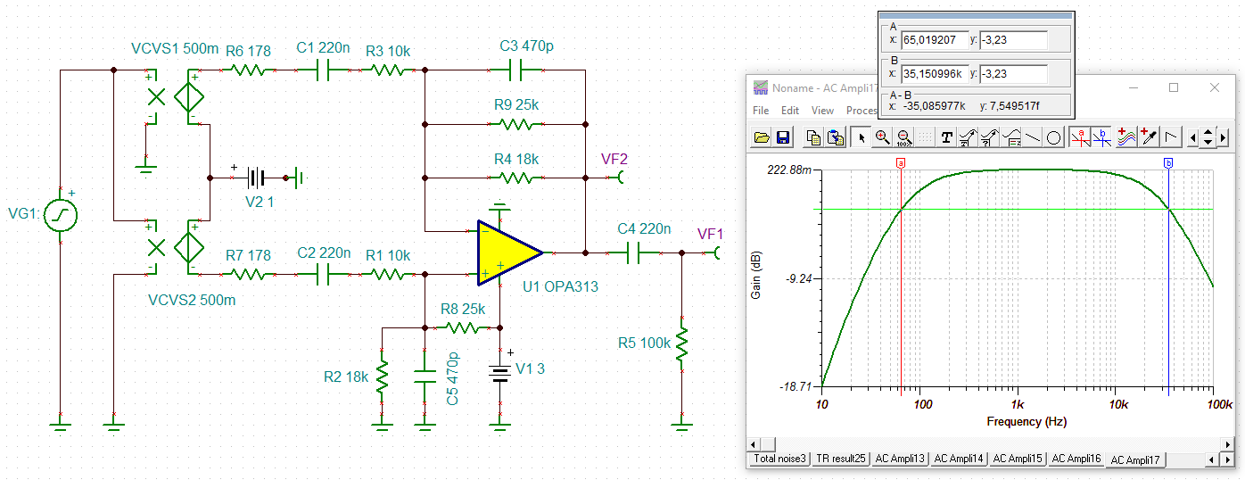
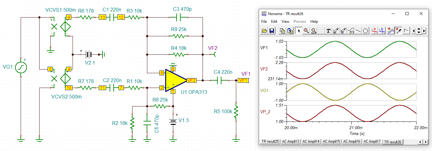
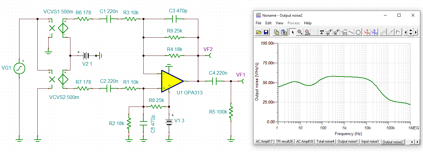
the CR2032 doesn't allow an all too high supply current. So I would choose a mircopower OPAmp. The OPA313 is rather low noise:
Kai
Suzuki-san,
Please let us know if any of the responses resolved your issue by pressing the green "resolved" button on the answer that resolved your issue.
Best,
Jerry
Dear Kai-san,
Thank you reply.
I understand that OPA313 has an advantage over OPA344.
The problem is that board I make is extremely simple.
Specifically, the board I manufacture does not have space to mount a regulator that produces V2_1 and V1_3 from CR2032.
If you have the idea of providing me with useful information, I expect you to consider the following:
Additional parts such as regulators cannot be mounted.
Only partial pressure using a resistor can be mounted on CR2032.
Gain = + 3.3dB, HPF = 194Hz, LPF = 13kHz
Thanks,
S.Suzuki
Hi Shinya,
V1_3 and V2_1 are no voltage regulators. V1_3 is the CR2032 and V2_1 simulates the 1V common mode output voltage of microphone.
Kai
Dear Kai-san,
Thank you reply.
1
I reflected your advice in schematic.
Is my understanding correct?
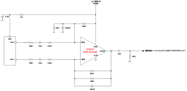
2
I think that OPA313 data sheet does not contain the formula for calculating the gain and HPF and LPF fc that correspond to circuit you propose.
Please tell me concretely and kindly formula to calculate gain of circuit you propose and fc of HPF and LPF.
Thanks,
S.Suzuki
Hi Shinya,
the parallel resistance of 30k and 22k is 12k7. The corner of low pass filtering is 1 Hz / (2 x pi x 12k7 x 1n) = 12.5kHz. The corner frequency of high pass filtering is 1 Hz / (2 x pi x (8350 + 178) x100n) = 187Hz. And the gain is 12k7 / (8350 + 178) = 1.49 which equals 20 x log (1.49) = 3.5dB.
To reduce the supply current of circuit choose C4 = 220n and R5 = 100k. And don't forget the isolation resistor R10 !
Kai
Dear Kai-san,
Thank you reply.
1
I reflected your advice in schematic.
Is my understanding correct?
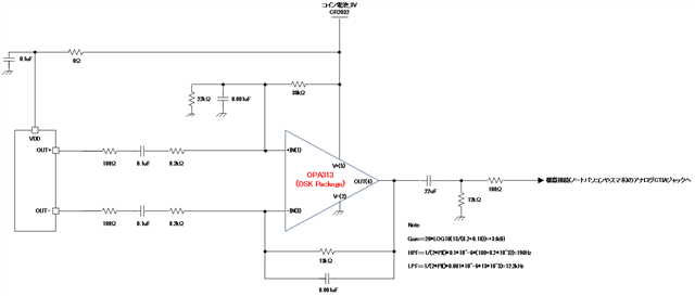
2
> To reduce the supply current of circuit choose C4 = 220n and R5 = 100k. And don't forget the isolation resistor R10 !
R5 is closely related to plug detection on smartphones or PC.
Therefore, I judge that 12kΩ is appropriate for R5 from viewpoint of plug detection.
Please tell me concretely and kindly impact that you do not adapt to C4 and R5.
Thanks,
S.Suzuki
Hi Shinya,
R5 is closely related to plug detection on smartphones or PC.
Therefore, I judge that 12kΩ is appropriate for R5 from viewpoint of plug detection.
Ok. But decrease the cap at the output from 22µF to 1µF then. The reason: 22µF can show a much worse distortion compared to 1µF.
The reason why I have chosen R5=100k is that R5 adds to the supply current drawn from the CR2032 cell when the output of OPAmp emits an audio signal.
I noticed that you have replaced the parallel circuit of R4=22k and R9=30k by a 13k resistor. But the parallel resistance of R4 and R9 is 12k7 and not 13k. Keep in mind, that for best common mode rejection R1 and R3, and R2 and R4, and R8 and R9 must exactly match. So replacing R4 and R9 by a 13k resistor will ruin the common mode rejcetion of this differential amplifier. You should find a better match.
Also, for optimum common mode rejection choose thin (!) film resistors of better than +/-1% manufacturing tolerances.
The same is true for C1 and C2. Choose caps with as little as available manufacturing tolerances. For the same rerason I originally have chosen bigger capacitances for C1 and C2. The bigger these caps the less their impact on the common mode rejection.
Kai
Dear Kai-san,
Thank you reply.
I reflected your advice in schematic.
I would like to know resistance value of R2 and R4, and R8 and R9 where the parallel resistance is 5.6kΩ.
Please give me a concrete and kind answer.

Thanks,
S.Suzuki
Shinya-san.
The values depend on desired DC output voltage. For mid supply, it is simply 10.2k for all four resistors.
For any valid DC Vout, the reverse Thevenin tab in the Excel spread sheet download can calculate values.
Rounding values to standard 1% choices will slightly change nominal gain and DC output voltage.