This thread has been locked.

If you have a related question, please click the "Ask a related question" button in the top right corner. The newly created question will be automatically linked to this question.

LMP7721: How to build a charge amplifier with fC resolution and low bandwidth?

Part Number: LMP7721
Other Parts Discussed in Thread: TINA-TI, OPA210, OPA928, OPA928EVM

Hello, 

I am not an electrical engineer but a chemical one. Therefore, my question is probably foolish/basic.

I would like to build a circuit that is able to measure the fC charge that is induced by a single particle flying through a Faraday cage. The particle will stay in the faraday cage for approximately 0.1 to 1 second.

On the internet, I found that I should use a transimpedance configuration of an op-amp, use a Faraday cage (grounded thin aluminum foil), and I should put condensers close to the power supply pins of the op-amps.

My idea was to use one LMP7721 as inverting charge amplifier and the second one as inverting voltage amplifier. And the Third one is a voltage follower of the output of the first amplifier so I can get larger gains on the second amplifier, The output of the voltage follower is filtered from the signal and passes only the offset voltage (caused by the bias current?). This works in TINA-TI, but not in reality. The output does not desaturate. Can you guide me on what I did wrong or if I should use a completely different circuit to achieve what I want?

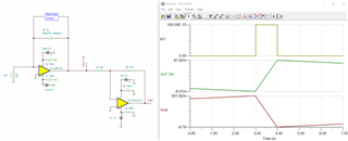
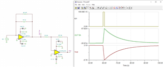
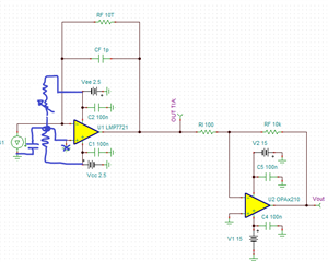
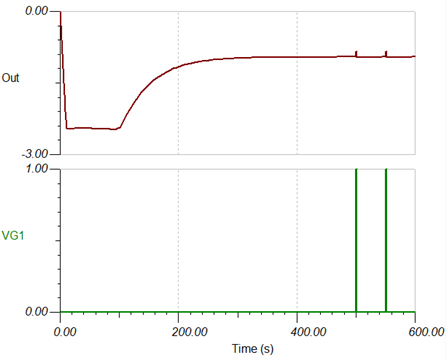
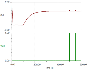
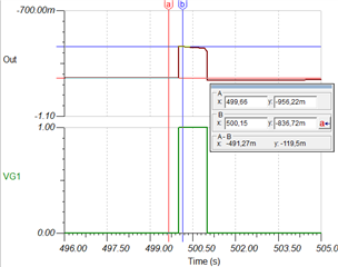
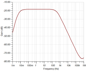
Below is my TINA-TI model. The VG1 and C1 should simulate the induction caused by the charged particle flying through the faraday cage. Next, I attached a transient simulation; the idea is that I will let the circuit stabilize. After the stabilization, I can inject the charge of 100fC (increase the VG1 voltage), and this will translate to a 100mV response on the output, which I can measure. The last image is a gain which is constant for my frequency.

I am able to make this circuit work for a resolution of 10pC when I remove the voltage follower and connect the non-inverting input of the U2 to the ground and tune down the gain on the U2. But I need those 2 orders of magnitude to achieve the required accuracy.

Since it is important for me to know how much charge was on the particle during the entrance and exit from the faraday cage, and the problem with the first amplification stage is that I need to use a large capacitor (C2) to keep the stability, which lowers the gain. Would it be possible to somehow sample the charge only during the entrance and exit? This would shift the bandwidth to higher frequencies which would allow a decrease in the value of C2, thus increasing the gain by those few magnitudes that I need.


I would upload the TINA file if I knew how.


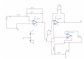
  •   Here is TINA-TI schematics, I forgot to upload it

  • Hi Simon,

    Resolving femto-coulombs of charge is certainly not a basic question.

    The transimpedance (TIA) configuration you have attempted to implement does not measure charge, rather it measures the instantaneous current flowing across your 10GΩ feedback resistor. With the 47nF capacitor in parallel your bandwidth is something like 300µHz which means you can only measure DC current in your circuit such as the input bias current (Ib) of the amplifier plus any parasitic "leakage" currents that are flowing into the measurement node on your board. 

    The charge Q accumulated on a capacitor is defined by Q = C*V where C is the capacitance and V is the voltage across the capacitor. If you want to measure 100mV for a given charge of 100fC, or in other words a gain of 1 Volt / pico-Coulomb, this will require a 1pF feedback capacitor (CF) in an integrator configuration. The integrator is similar to the resistive TIA, except the input current charges the feedback capacitor over time, resulting in a ramping output voltage which represents the total charge accumulation.

    The equation for charging a capacitor is I = C*dV/dt. So, if you are expecting 100mV accumulating across a 1pF capacitor in a measurement period of 1s, the input current will be in the range of 100fA. The LMP7721 is a good choice as its input bias current (Ib) is typically 3fA at room temperature. The Ib and leakage currents present as a DC error in your system and these errors should be measured and calibrated out of your final results.

    The circuit below uses the LMP7721 in an integrator stage, followed by a gain stage. Note that the OPA210 in the gain stage can use a wider power supply than the front-end stage which allows for greater measurement resolution at the output. In this configuration, charge continues to accumulate on the capacitor over time due to Ib which will eventually saturate the output unless the capacitor is discharged. A specialized low-leakage switch must but placed in the feedback path that closes to discharge CF and opens before a measurement is taken.

    The circuit below uses the LMP7721 in a "leaky integrator" stage, also known as a charge amplifier. The second stage is a gain stage using OPA210 and is the same as in the above circuit. The 10TΩ feedback resistor (RF) allows the output to settle to a DC value defined by the Ib and leakage currents flowing across RF. In simulation, Ib of LMP7721 is 3fA and the output of the LMP7721 settles to ~30mV. The settling time is defined by the RC time constant of RF and CF. 10TΩ was chosen for RF because it makes the RC time constant much greater than the measurement period of 1s. If the time constant is not greater than the measurement period, CF will discharge before the total charge can accumulate and the measurement is compromised.

    When dealing with femto-amp level currents in the real world, nothing is as simple as simulation. PCB layout and cleanliness is of extreme importance as parasitic current paths through PCB material and surface level residues can be hundreds of pico-Amps, completely degrading the measurement. Large RC time constants caused by high resistance values and parasitic capacitance can result in discharge times of hours or even days. The LMP7721EVM User's Guide has helpful information on PCB layout and cleaning the board after assembly. I would recommend starting there: LMP7721EVM User's Guide.

    We also have a new femto-amp input bias current device OPA928 that will be launching very soon and has higher performance than LMP7721. The OPA928 allows power supplies up to +/-18V and features an internal guard buffer that can be extended to guard against current leakage on the PCB. The OPA928EVM User's Guide will have detailed information on the low-leakage switch required to discharge the integrating capacitor.

    Regards,

    Zach

  • Hi Simon,

    can you tell more about your set-up?

    What particle and what charge are we talking about? Is the charge moving in air or vacuum? Why is it moving so slowly? Where does the charge come from? Usually, a slow charge is immediately captured by the surroundings. How do you prevent this?

    Do you know the Millikan experiment?

    Kai

  • Thank you, Zach. You helped me tremendously. Using OPA210 and the user guide you sent can solve most of my problems. If this would not work, I can wait for the OPA928. 

    However, I have two questions.

    1) You mentioned, "The Ib and leakage currents present as a DC error in your system and these errors should be measured and calibrated out of your final results." How can I achieve that in the leaky integrator stage? I would like to use this configuration because it best captures my experiments' nature. Using your second figure. Can I offset the noninverting input to the U2 so that the voltage difference between inverting and noninverting input is zero when no signal is supplied? Can I use a voltage divider with a potentiometer to fine-tune the offset of 30mV from, for example, a 2.5V voltage reference for this purpose (~93k and ~1.1k)?

    2) Do I need to implement some overvoltage protection of the input to the amplifier, especially the second one? The input of the second amplifier can be potentially +-2,5V volts given by the LMP 7721 supply voltage. In the Datasheet (of OPA210) on page 4, a Voltage Signal input pins Differential is specified to be 1V (see the fig below). I am unsure if this refers to the differential connection of the supply voltage (i.e., V-=GND) or voltage between input pins,i.e.,( ||-IN| - |+IN|| ) ?

    If it is the latter case, can you suggest to me a user guide, handbook, etc.. which tackles this problem?

    Thank you again

    Simon

  • Hello Kai,

    My setup aims to measure the transferred charge during a collision of powder particles (Triboelectric effect). Therefore my particles are quite large, from 20um to 1mm, and carry a small amount of charge, which makes a charge-to-mass ratio small. This limits the unpredictable trajectory because stray electric fields do not significantly influence them. However, this also limits the usability of the Millikan approach since I need to work in atmospheric conditions where the maximal value of the electric field is limited to around 3MV/m. However, according to my back-of-the-envelope calculations. If the rise velocity is infinite, i.e., Fg=Fe. I can use this approach to measure a particle of up to 150 um (it does not cover the whole experimental range) when the particle's charge is 100fC and particle density is 2 100kg/m3. It is linearly dependent on the charge and the third power of particle dimension.

    I shoot particles on the target, where the triboelectric effect occurs (some charge is transferred). This target is enclosed in the faraday cage, which I use to measure the charge of the powder particle before the impact on the target (the initial rise of current), and when it leaves the faraday cage (the reverse current). Because the system is in the integrator setup, I can evaluate the initial charge of the particle (the initial step) and the transferred charge (shift in the baseline). Because I am shooting the particles, the target is quite large (so I can hit it); thus must be the Faraday cage. I am working in atmospheric conditions; therefore, the settling velocity of particles is relatively small. Those two things impose the requirements on the RC time constant of the integrator, which must be pretty large.

    Simon

  • Hi Simon,

    Zach is out so I'll cover for him this week.  In response to your questions above:

    1) Yes, you could certainly calibrate out any error in the system at a single temperature with a potentiometer-type solution you mentioned, similar to below:

    I have shown above 3 resistors, two fixed and one potentiometer.  The potentiometer will fine-tune the offset - if you only use 1 resistor and 1 potentiometer, you may not have enough resolution to dial-in the offset. Ideally the values of these resistors are low, I would suggest in the range of 1 kOhm, the reason being that the noise of the resistors will directly impact the measurement.  For this reason you will also need for capacitance to ground to help filter noise effects.  Also, you may be able to calibrate at a single temperature, but, this does not include any shifts that are associated with temperature change.  Also, depending on the 

    2) You should not need any additional resistance; the limit you mention above is specifically referring to the input terminals, that should nominally be at the same voltage.  The inputs can have situations where they become separated, but that typically only happens when the amplifier encounters an open-loop situation (i.e. the output hits the supply rail). Even in this case, the inverting terminal resistance will help limit the current.  But, in the inverting configuration above, the amp. will always for the inverting node to GND so there should be no differential voltage on the inputs with the exception of the offset and bias current errors, which are very low for this amp.

    I hope this helps.

    Best Regards,
    Mike

  • Hi Simon,

    this sounds very interesting and is far away from any standard application Relaxed

    Because of the very large time constant of integration and the small charge, wouldn't it be a good idea to do all the integration in software? This would allow you to simply your circuit. You would focus on building a proper TIA and would get rid of all leakage current issues of integrating cap and optional discharging switch. Only an idea...

    Kai