This thread has been locked.

If you have a related question, please click the "Ask a related question" button in the top right corner. The newly created question will be automatically linked to this question.

JFE2140: DC from JFE2140 Composite Amplifier

Part Number: JFE2140
Other Parts Discussed in Thread: OPA604, OPA202, LME49860, TINA-TI

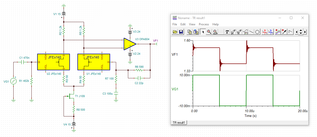
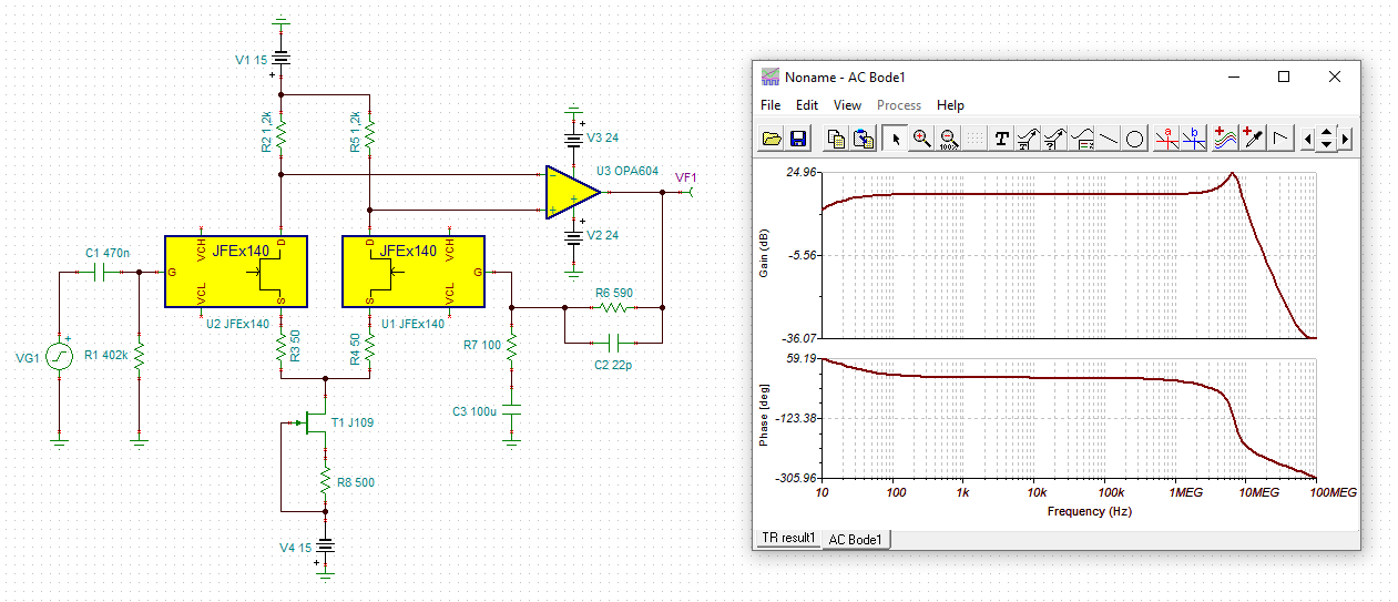
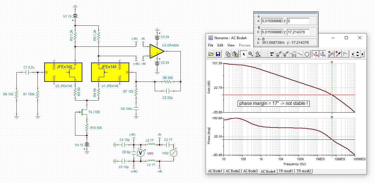
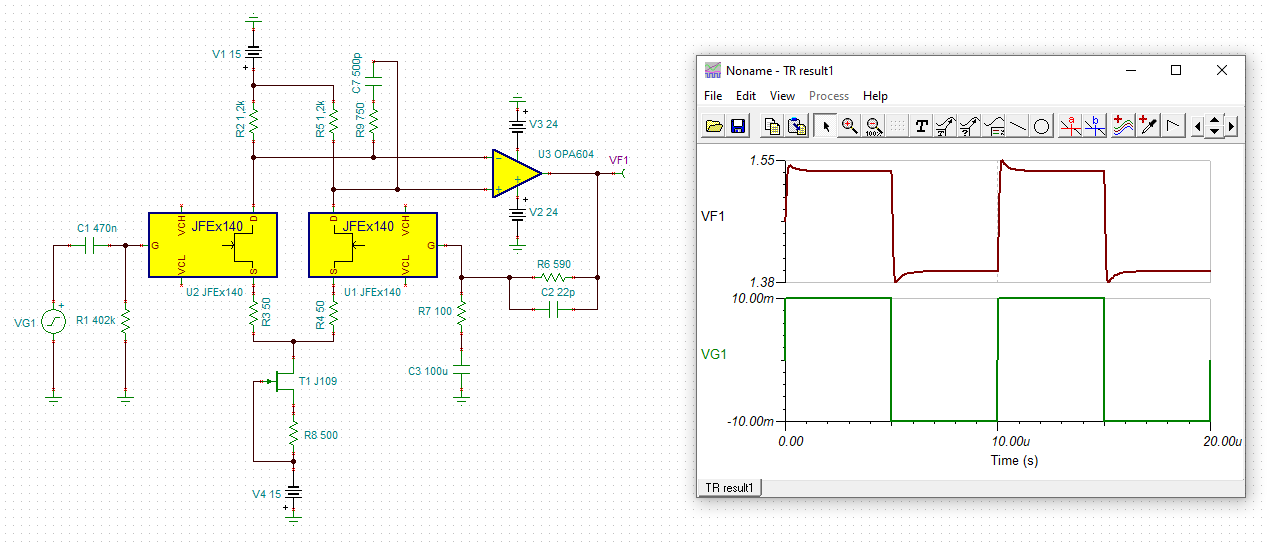
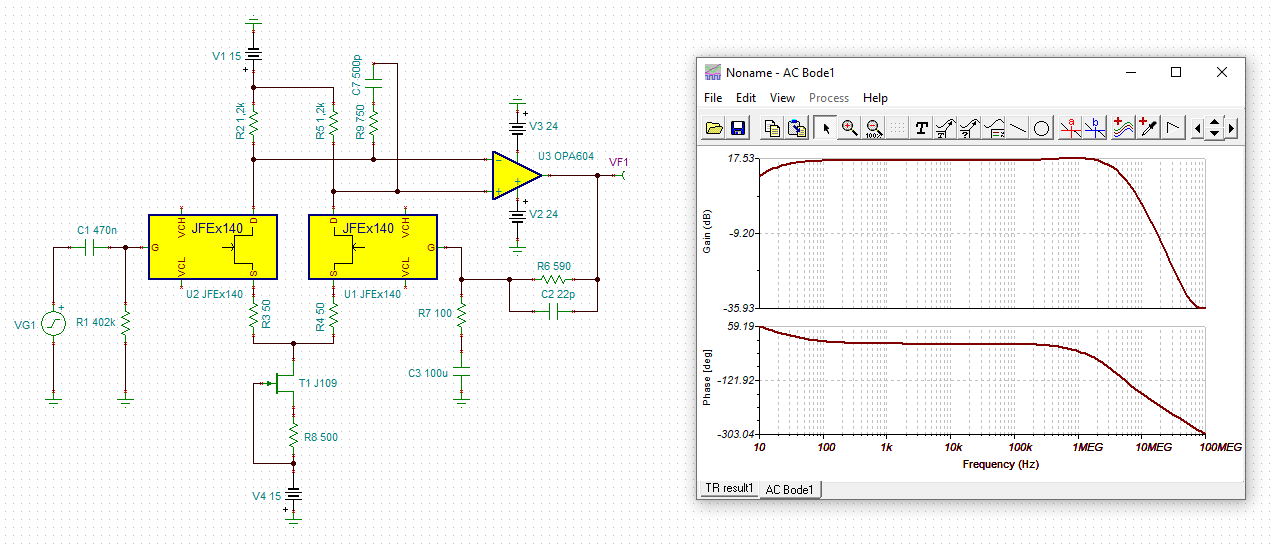
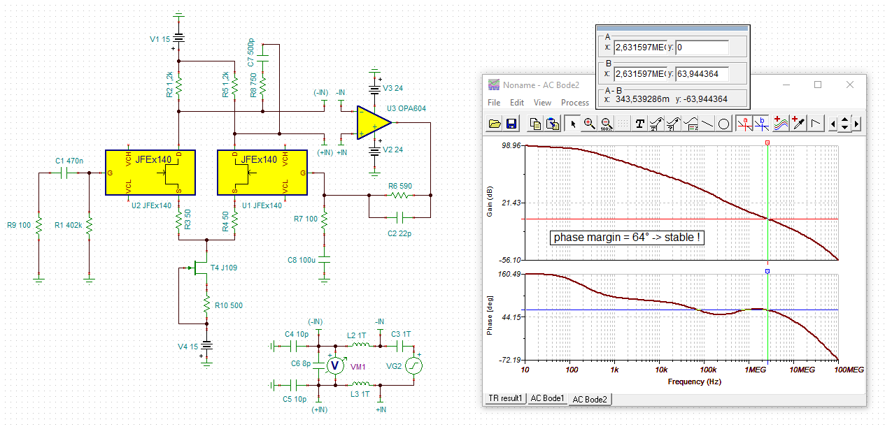
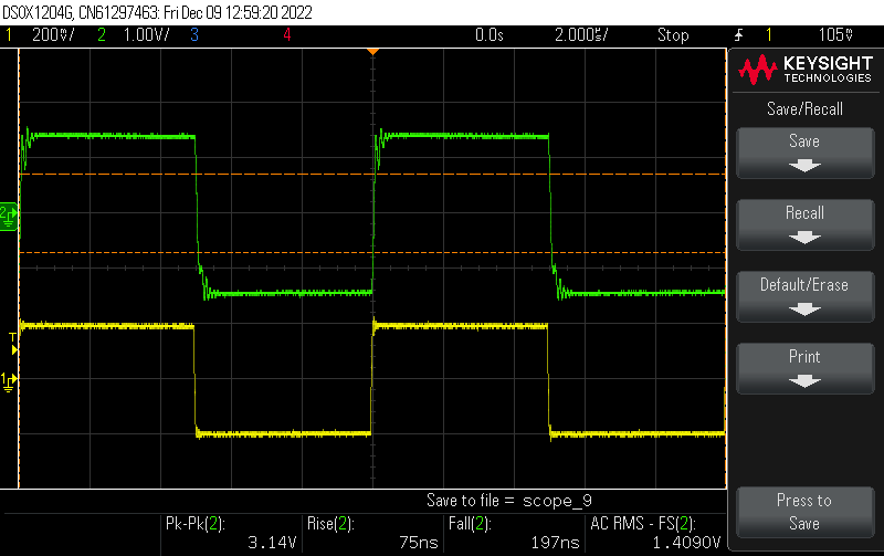
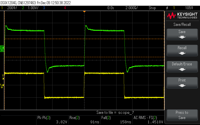
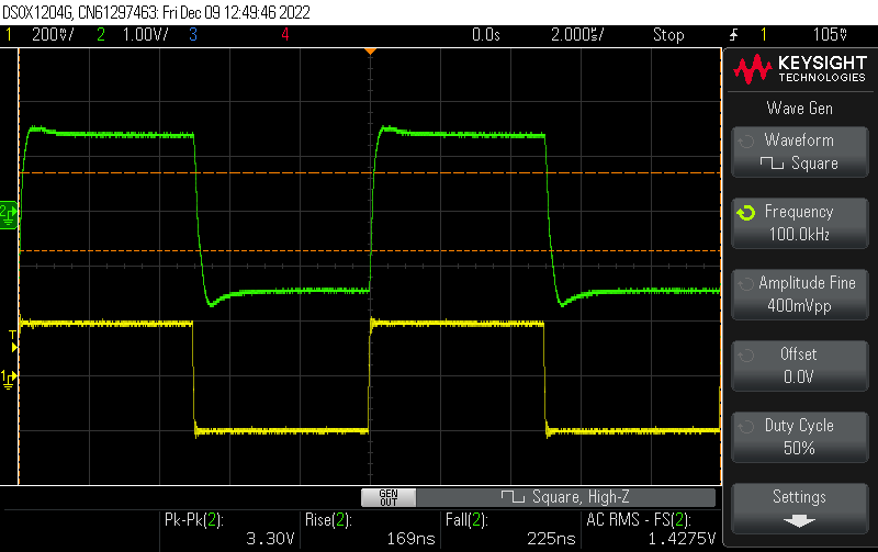
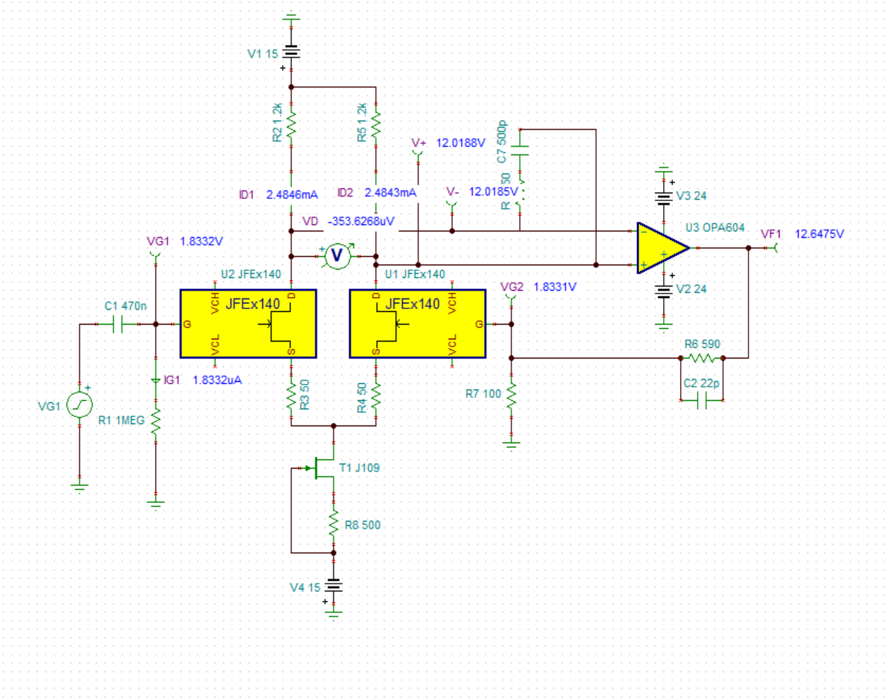
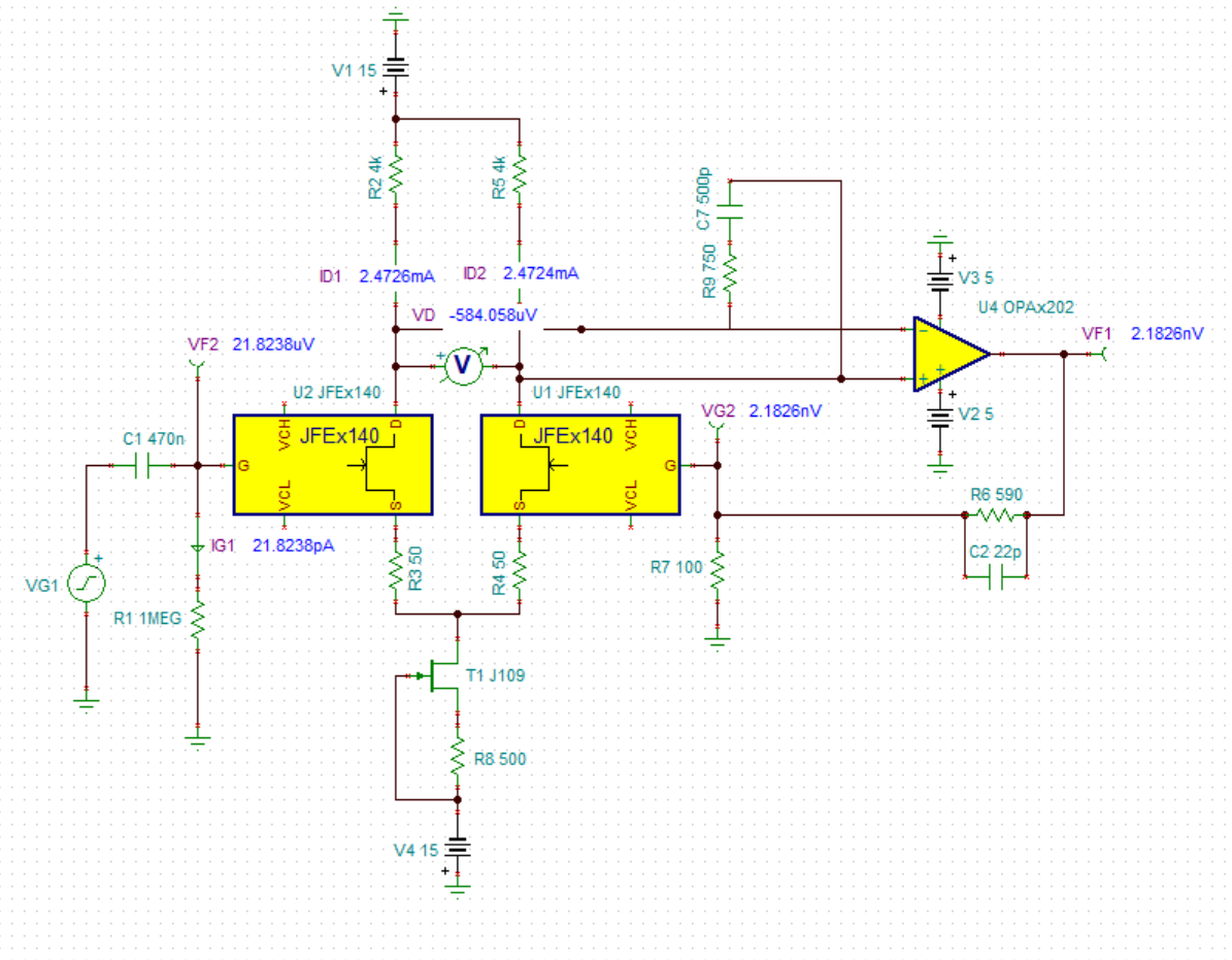
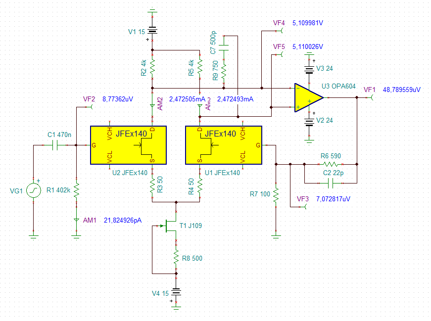
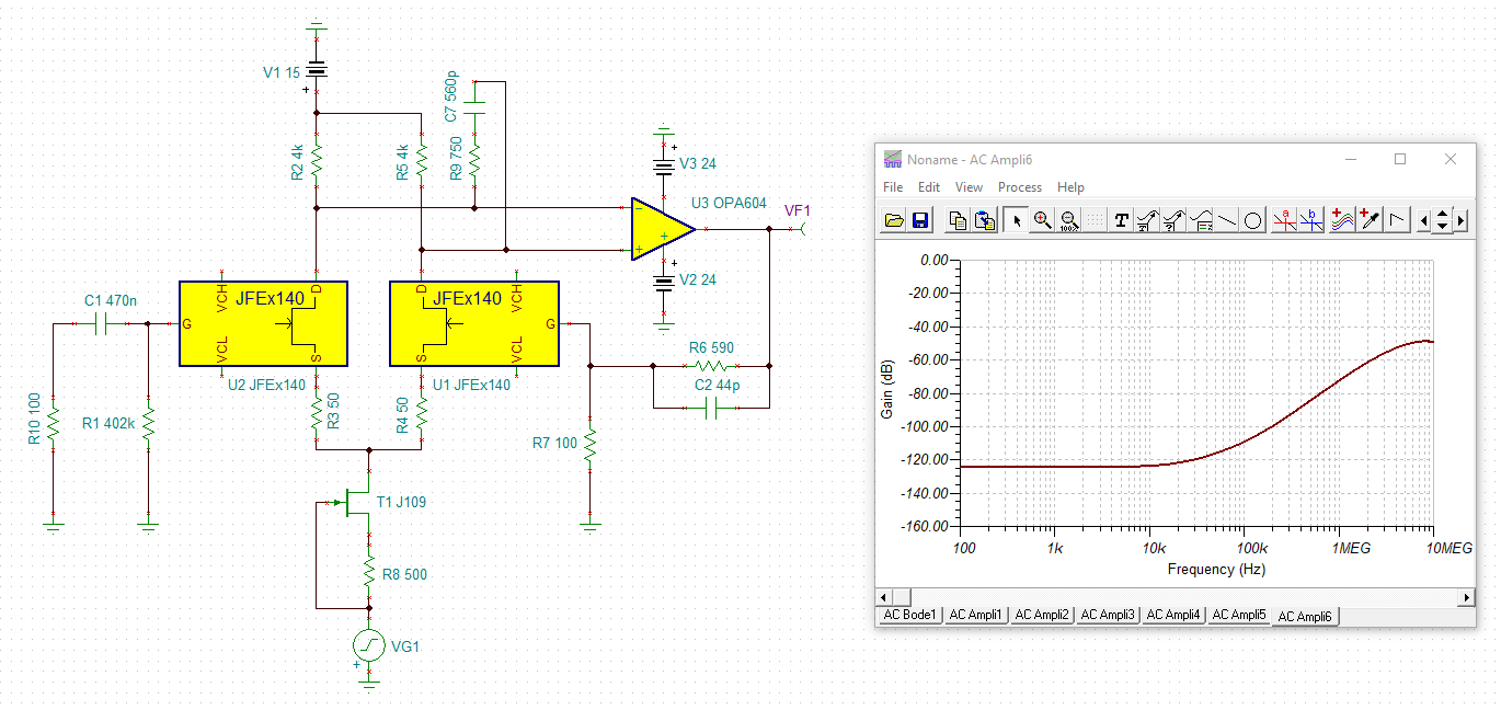
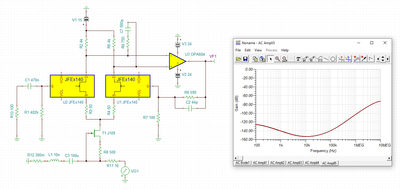
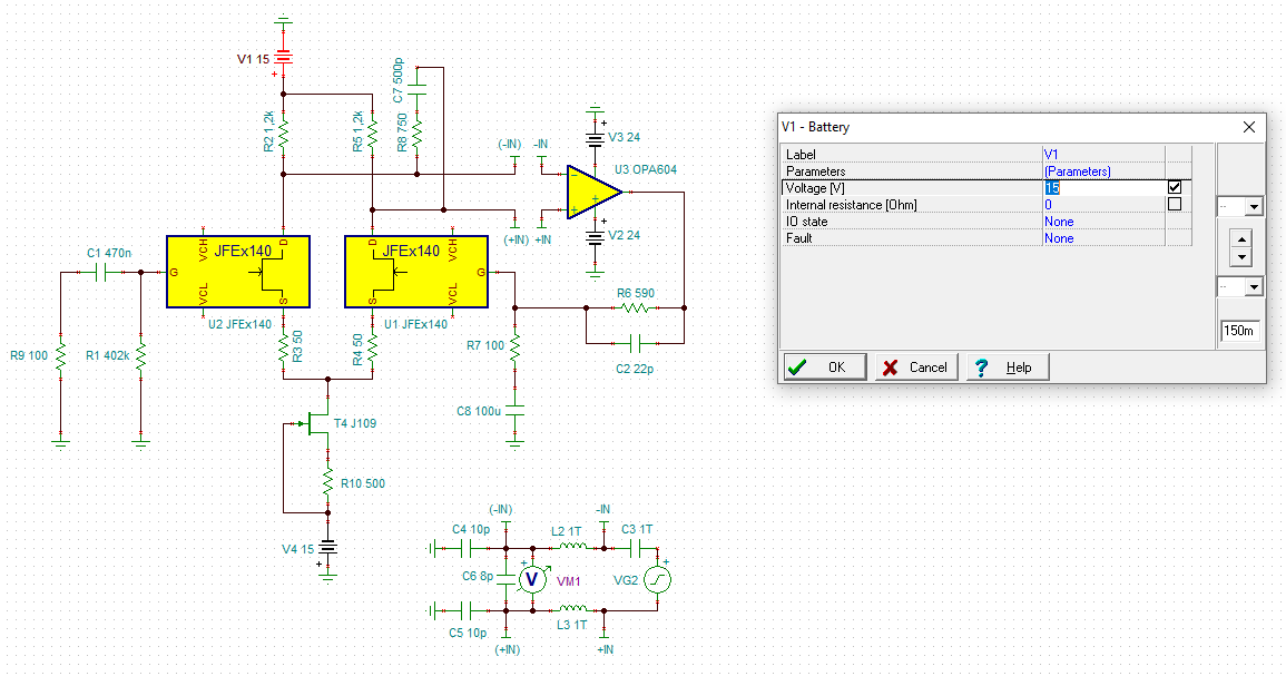
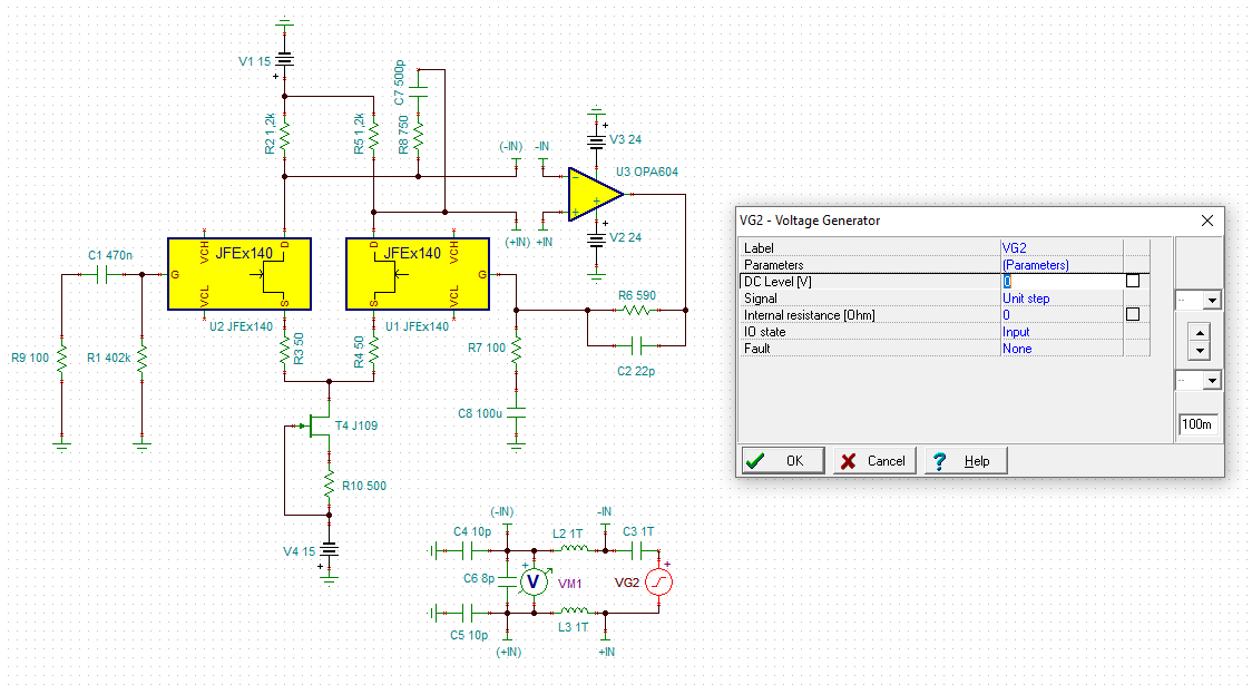
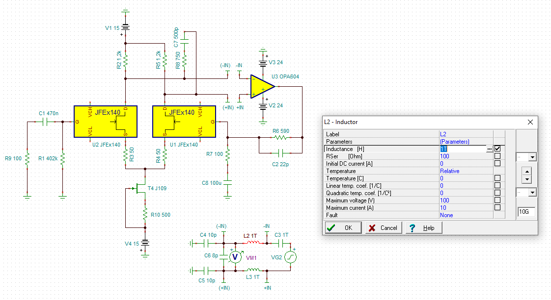
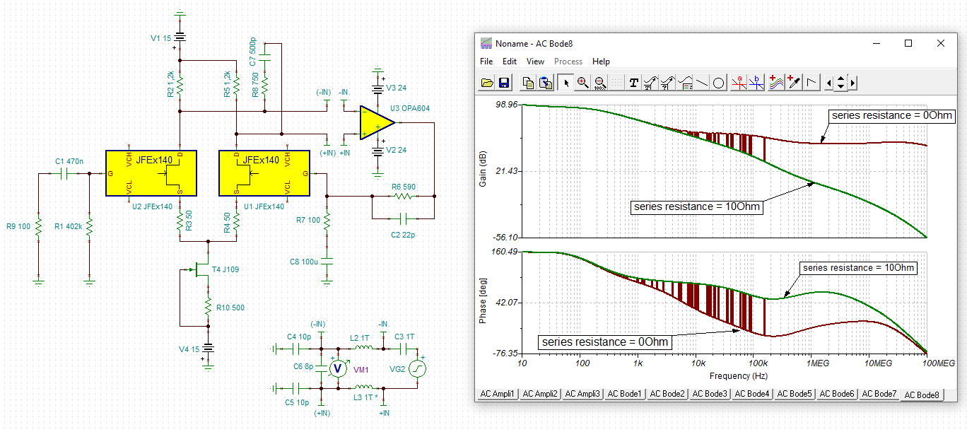
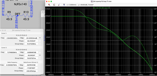
I've built a composite amplifier using a JFE2140 dual JFET and a OPA604, similar to Fig. 9-6 on the JFE2140 DS. Two that I've built work fine, but two others exhibit DC gain. As the input is increased, the DC output goes positive. When I tested the first one that had this, I thought there must have been a wiring error I couldn't locate, until I built another with the same problem. I've exhausted my ability to troubleshoot these two problem samples. LTSpice does not show anything amiss. (I don't believe PSPICE-TI supports my Mac OS, but please let me know if it does.) 

The total gain should be about 7, and I have an input blocking cap, so that the only DC at the input of the first JFET gate should be due mostly to imbalance in the circuit. By the time the input AC signal is 1 volt RMS, there's more than a volt of offset at the output, however. 1.75V peak at the input signal results in 5.4V DC output.
 
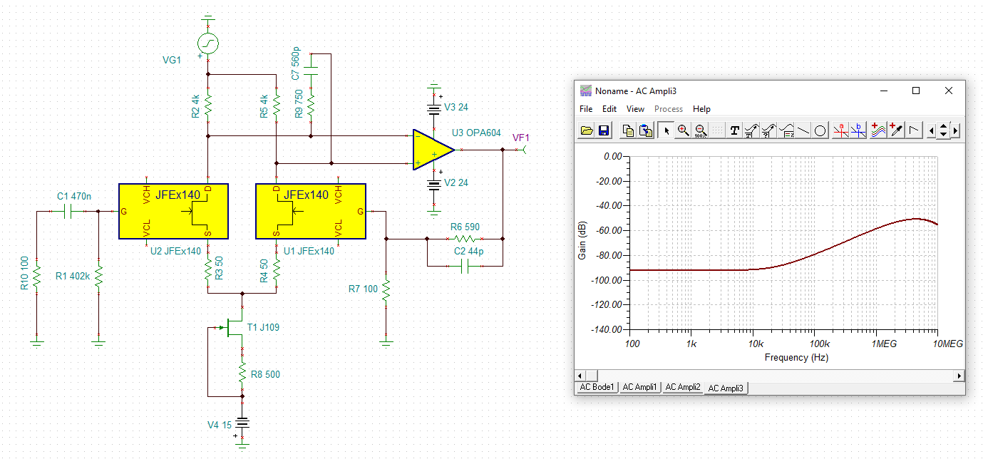
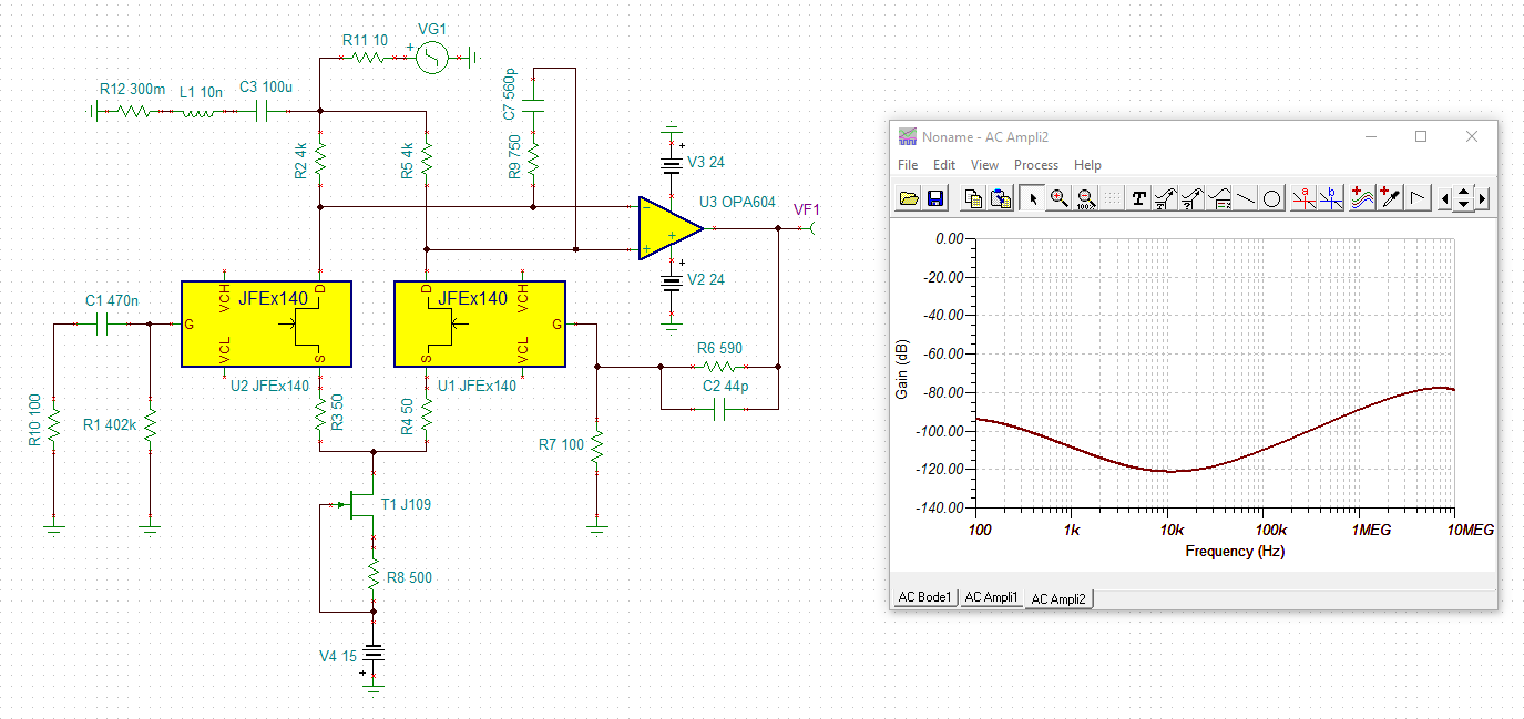
A schematic follows.

What am I missing? Thanks in advance.

jfet opamp fb.pdf


  • Hi Charles,

    JFETs come with huge manufacturing tolerances. There's a certain probability that your circuit runs away from the wanted operating point.

    1. Can you measure the voltage drop across R4? You can adjust the current through the JFETs J1 and J2 by modifying R4.

    2. When the constant current programmed by R4 and J3 becomes too small, the voltage drop across R5 and R7 can also become too small and the input voltage of OPA604 may leave the common mode input voltage range. So please measure the voltage drops across R5 and R7. What is the supply voltage of OPA604, by the way?

    3. The circuit could be instable. Have you already performed a phase stability analysis? See this thread, for instance:

    https://e2e.ti.com/support/amplifiers-group/amplifiers/f/amplifiers-forum/1080422/jfe2140-jfe2140

    Kai

  • Thanks, Kai!

    1. On my as-built circuit, the constant current source J3 is a J109 selected for its IDSS and R4 is 590 ohms. I'm measuring 2.902V across R4 for 4.92mA for both JFETs summed. (I wonder if there could be a power-up problem, but can't think what it would be.)

    2. R7 drops 2.837V (2.40mA) and R5, 2.975V (2.52mA). That leaves a hair over 12V at each input terminal to OPA604. +Vcc for the op amp is 24V from a L78L24 LDO, and -Vcc is normally -23.5V from an adjustable LDO off board. So my Vin CM range should be at least within 3V of Vcc or well above 12V. Just in case 12V is an absolute regardless of rail voltage, I tried increasing R5 and R7 to lower those input voltages, but there was no improvement.

    3. I will need to spend some time to check stability, which I can't do till Monday but I will report back. (I missed most of the posts on that thread, though I had seen at least one in a general search.)

    Thanks again.

  • Hi Charles,

    it turns out that your circuit is instable:

    Because of convergence issues of simulation I had to decrease R1 from 402k to 100k for the phase stability analysis. There's a know bug in the SPice model of JFE2140 generating a way too high base current. This not only results in a huge offset voltage in combination with a high source resistance but also has an impact on some of the simulations. But your circuit is still instable.

    You should add a phase lead compensation as shown below:

    charles_jfe2140.TSC

    charles_jfe2140_1.TSC

    Yes, latch-up is a serious issue of this circuit. Two things can decrease the risk of latch-up:

    1. Power the whole circuit from only one bipolar supply voltage. This avoids issues resulting from uneven power-ups.

    2. Choose a high gain in the feedback loop for all frequencies. Omitting the 100µF AC coupling cap may help. The JFE2140 is such an ultra low noise JFET than operating it at a low gain makes no sense. For low gain applications a low noise OPAmp can be better used.

    Also see this very nice appnote:

    LSK489appnote.pdf

    Kai

  • Kai,
    Let me digest this a little before testing and getting back later. I've been mostly thinking about the latch-up since Saturday, having been away from my bench. In testing I did see the peakiness and added 44pF between the output and the negative terminal of the op amp. It smoothed out the response, but I should compare it to the network you added. I didn't show it on my schematic, because it's not on the DS app note and thought it was mostly a red herring to the DC issue.

    Thanks for doing the analysis and showing these results. I need to learn how to analyze stability better, and this will help. I've generally gotten away with testing in closed loop and adding a single pole, like I did with the 44pF, until the response and square waves look good.

    I'll get back with findings, but thanks again for now.

    Charles

  • Hi Charles,

    you may want to watch this TI's training video series of stability:

    https://training.ti.com/node/1138805

    Kai

  • Charles,

    Agreed with Kai's stability analysis.  There is one thing that needs consideration here from a DC perspective; the JFE2140 will have current flow into the gate for higher VDS voltages, similar to any JFET.  This is generally referred to as impact ionization, it is dependent on the Vds voltage as well as the ID current, see the chart below:

    I would have expected to see some difference even in the DC-bias conditions, so I am not sure about the mechanism of how this relates to the DC offset increasing with amplitude.  But I could see how this becomes worse if the amplifier is no longer able to maintain constant Vd voltages.  Ideally, both input nodes of the op-amp stay the same (assuming the loop gain is high) but if there is a condition that forces the drain nodes to separate (i.e. Vds gets too low and the JFET goes into triode), then there can be larger swings on the Vd node.  When this occurs, the gate current can become rectified and potentially look like a DC offset.  See the basic simulation below, where Vd is varied from 7 to 17 V, the gate current is almost zero when Vd is low, then increases as Vd increases.

    If you increase R7 and R5, this will effectively lower the Vds voltage, and increase the gain from the JFET stage.  Can you double those resistors and see if the problem is improved?  Also taking into account Kai's stability suggestions.

    Regards,
    Mike

  • Thanks, Mike. I think that might be closer to the issue, but I'm now just trying to deal with my test platform. I need to get it back to a baseline after some rework and other kludge issues have kept me from moving forward. I think power-up is also part of the problem.

    Once I get my previously working configuration back up and going to where I can do measurements, I'll check this and stability. However, I'm still thinking the compensation I added was sufficient for stability; I just need to get the circuit back on my bench to get those numbers, which I'll post here. TBD...  

  • Hello Kai,

    I've had a chance to test some more, starting with one of my working units.

    Stability: My 44pF from output to negative input terminal does come with a slight peak at ~2.5MHz, but it's much reduced in amplitude from the passband. There is a little bit of ringing on the input signal due to mismatch from generator, too, so some on the output may follow from that. (I used 400mV p-p input, to get something clean.)


    Your suggested compensation looks like this at 100kHz (I used 560pF that I had on hand + 750 ohms):


    Using both my 44pF local and your input network (both in addition to the 22pF FB cap) produced the best looking result:


    This looks like the way to go! However, no compensation that I added (or none at all) provoked the DC problem I see with two other units.

    1. (Supplies). My supplies are coming up at about the same time.
    2. I'm not using the 100uF DC unity gain cap. That was just in my LTSpice circuit with a short around it. Also, one of the reasons I chose the OPA604 is that I need at least 44V across the op amp to get the amplitude needed. It, of course, is among the vast number of good op amps not in supply now, though it was in small supply when I started this earlier in the year.

    Next, I will go back to the problematic board to re-examine the DC behavior.

    Comments welcomed, but thanks again,

    Charles

  • Hello Mike,

    On a good unit that does not show the problem, I have about 11.6V Vds across the JFETs. That should correspond to <10nA from your chart, which should yield about 4mV DC across my 402k ohm resistor. Best I can measure is about 2mV with an AC signal present.

    I'm going to test one of my bad boards some more to see if I can narrow the source of its problem. I first needed to get some more parts, but now have those.

    Thanks,
    Charles

  • Hi Charles,

    looks very nice now Relaxed

    Kai

  • Hello Charles, 

    I have been looking at the design inside of Tina Ti. I am trying to narrow down the issue for the DC voltage you are seeing. Can you measure the Vgs voltage that you are seeing on a board that exhibits high DC values on the output? My suspicion is that the CMRR of the OPA604 of 80 dB or 10mV/V is to blame. I have two simulations below. One is using the OPA604 and the other is using the OPA202 as the composite amplifier. I believe what may be happening is that the OPA604 is biasing the JFET on the beta network side with a positive VGS. This may be re-biasing the circuit away from expectations. Using the OPA202 I do not see this issue. The CMRR performance of the OPA202 is significantly higher with 146dB typical. Please see below. The gain is low enough where I do not expect the Vgs mismatch to create this DC value. If you can measure the gate voltages this to see if it aligns with what I am seeing in simulation it may help us narrow down the issue. 

    Best Regards, 

    Chris Featherstone

  • Hi Chris,

    good catch Relaxed

    Increasing R2 and R5 in the existing design from 1k2 to 4k would also do the trick, at least in the simulation:

    charles_jfe2140_2.TSC

    From the beginning I had the feel that 1k2 is a bit too small. Because of you I know why now...

    Kai

  • Hi Charles,

    there's another trick which is often used in such discrete operational amplifier circuits, the use of RC low pass filtering in the supply lines. One positive effect is that the circuit has more time to settle to the operating point and by this can better stabilize. Provided that also the supply voltage lines of OPAmp are filtered, this can very effectively prevent latch-up in the JFET stage caused by unwanted output voltage glitches coming from the OPAmp.

    Another advantage is the enhancement of power supply rejection of the discrete JFET stage as shown below:

    charles_jfe2140_4.TSC

    In this example the effect of a 10R / 100µF (aluminium electrolytic) low pass filter is shown. L1 and R12 simulate the self inductance and ESR of aluminium electrolytic. Of course, a 100...470nF / X7R can be mounted in parallel to the 100µF cap to enhance the filtering at higher frequencies.

    Below the effect in the constant current path is shown:

    charles_jfe2140_5.TSC

    The positive effect of the constant current source on the power supply rejection can clearly be seen. Nevertheless, even the constant current source source will profit from RC low pass filtering at the higher frequencies, because unwanted junction capacitances within T1 will minder the PSRR at higher frequencies.

    10...100R and 100...220µF can usually be seen in such circuits.

    Kai

  • Hi Chris,

    I JUST FOUND THE PROBLEM! I disconnected the negative clamp diode connection VCL from ground and that eliminated the DC.

    Here's how I got here: I built three units on proto boards, not intending to connect the ESD terminals at all, but one out of the 3 showed this problem. Not ever finding the issue, I assumed there was a mis-wire somewhere. (I had swapped out op amps and JFETs, unsuccessfully, and that board got messy to work with.) Confident that the design was okay, I layed out the board and had some made (my first use of KiCad and PCBs from OshPark).  Churning again through last night, I remembered these pins might be different from my proto boards. I meant to disconnect VCH, but cut VCL trace by error. But that was enough to make the problem go away.

    Apparently a lot of capacitance from the steering diodes was coupling to the gates. Why would this be? Problem solved (I THINK), but not fully resolved/understood. (EDIT: I get it; diodes would be turning on, as intended.) I can check the box as resolved if you'd like, but would like to get your inputs first.

    Below is my KiCad schematic, BTW. It doesn't include Kai's RC network that improves the stability, which I'll add. You or Kai may wish to comment on my choice of regulators and filter caps, the polar ones of which are all aluminum polymer types.

    Also, I had changed R2 and R5 to 1770 ohms, without improvement, but I will consider larger ones and the CMRR situation as possible improvements. If I get some more PCBs, I may also change the op amp to a dual to utilize an LME49860, which I have a few of and will handle the output swing needed.

    Passworks VFET FE copy.pdf

    Thanks for your time and advice,
    Charles

  • Hi Charles,

    connecting VCL and VCH to unsuited potentials can indeed be the cause of your DC issues! I would connect pin 7 of JFE2140 to -15V and pin 3 to +15V, according to figure 11-1 of datasheet.

    And I would use only one +15V regulator for both drains. A zener diode or a resistor between the +24V and the input of +15V regulator will help to reduce the heat dissipation of +15V regulator, if this is the reason for using two regulators.

    And I would think about adding RC low pass filters in the supply voltage lines as already mentioned.

    Kai

  • And add an isolation resistor at the output of OPAmp.

    Kai

  • I understand it now. The gates need to go negative. Tying VCL to ground, which I did because I didn't want to get close to the 40V abs. max rating, allows the clamping diodes to turn on. Yeah, duh....  I think I might just leave them unused.

    I just used two 15V regulators because they're cheap and thought two in isolation would make up for their output impedances not being as low as a single, better regulator that I'd prefer to use when driving more than one load. I do realize that adds to DC offset at the input of the op amp.

    I will review that and all your other good tips.

    Thanks all very much!

    Charles 

  • Hello, Kai, and Happy Holidays to you!

    I just got my LTSpice Bode simulator to work fairly well, I think. To refine and cross-check it, can you share what the SPICE directives are for V and VG2 in your circuit above? (I can't use TI tools as they are Windows only; I'm thinking the same expressions should work in LTSpice, though. Maybe with some minor translation.)

    Thanks.

  • Hi Charles,

    the voltage sources "V" have a zero Ohm source resistance:

    "VG2" also has a zero Ohm source resistance. In TINA-TI the chosen input signal shape has no influence on the AC analysis. Here the "unit step" was chosen:

    To prevent simulation errors L1 and L2 have a 100R series resistance:

    This series resistance is sometimes necessary. 10...100R will usually do the trick:

    Wish you a Happy New Year Relaxed

    Kai

  • Thank you again, Kai. I deleted an earlier reply, so it can be disregarded. I wasn't able to run an LT Spice simulation using this method, but on further consideration there's no need to. I was curious to compare different simulation results, but it's really not necessary or very useful for what I'm doing. The two boards I have are working splendidly, with large help from your suggested compensation that I employed. One has less than 0.04% THD across the audio band up to clipping, and the other has somewhat less. This is much lower distortion than the output stage with which they're being used.

    So I'm done and happy. No further assistance is needed on this. Best to you.

    Charles

  • Hi Charles,

    can you post your LTSpice file here?

    (You have to zip it before attaching.)

    Kau

  • Sure! Can you use the native .asc files, or just PDF or images to see the schematic, etc.? I'll post the one that works and the new one that's missing something.

  • Here's a ZIP file of the .ASC files and PDFs. One uses LoopGain2.asc and the other I tried to duplicate your Tina TI generator without success. Also have PDFs of each and a screenshot of the results with the LoopGain2 technique. Note my curves are shaped a little different, but I got ~66 deg. P.M., about the same as you did.

    (These circuits omit the 44pF local op amp capacitance I originally had and which I found to improve stability further, when combined with your lead network.)

    Charles

    Dec30.zip

  • Hi Charles,

    taking a quick peek, I see two issues:

    1. Choose a sine wave for "Vi1" and set an AC amplitude of 1mV (different from zero !) to be able to perform a "small signal AC analysis".

    2. "Vi" must not be a "voltage source" but has to be a "voltmeter".

    Kai

  • Beautiful! Now it works. Curves look right. Need to compare to other method. Curves look about the same, but this is 70dB lower... Must be T only (AB)  as other was A (open loop)?  I'll look more closely later.

    Thanks and take care,

    Charles

    UPDATE: If I change Vi1 to 1.414V, I get something pretty close to your ACBode2 plot, at least for gain. ¯\_(ツ)_/¯


  • Hi Charles, 

    It looks like that you replicated the Tina simulation in LTSpice. I am going to close this inquiry.

    If you have additional questions, please let us know. 

    Best,

    Raymond 

  • That's a good idea, Raymond. Thanks everyone for all the help.