This thread has been locked.

If you have a related question, please click the "Ask a related question" button in the top right corner. The newly created question will be automatically linked to this question.

XTR111: I am not getting correct value in output of Xtr111

Part Number: XTR111
Other Parts Discussed in Thread: LM358, TLV2170, TLV9302, OPA2170, LM7705, TINA-TI

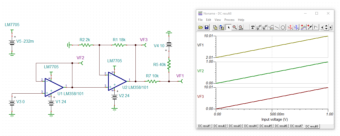
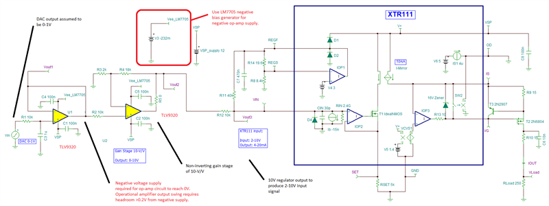
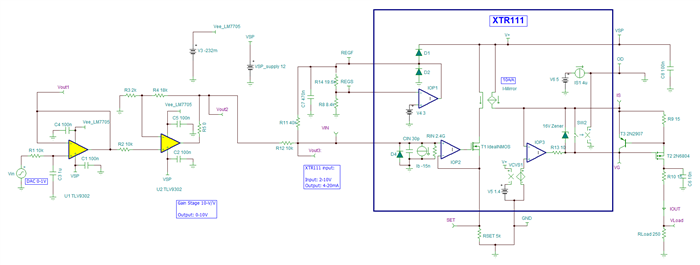
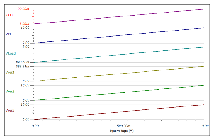
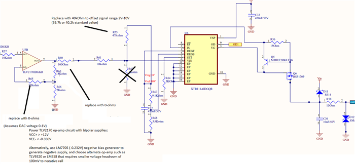
hello. I've been trying to get 4-20ma output with xtr111 for a while. I'm applying the output of lm358, which has a gain of 10, giving 0-10v output, to the input of xtr111 with a serial 10k resistor. However, When we apply 0v to the lm358 input, I measure 0.65v at the opamp output. Naturally, the output of xtr111 is greater than 4ma. Please help me to fix the problem.

  • This is my schematic

  • Hi,

    you could do it this way:

    Kai

  • thanks Kai.

    What's wrong with my circuit? Please can you answer? Why is the output of the opamp about 0.0015v when the opamp is not connected to the XTR111 and I apply 0V to the opamp input, but 0.65V when I connect it to the XTR111?

  • HI Elektroboard,

    I am unable to open your schematic pdf file. 

    The post above provides a link to a share box, and TI’s network access to cloud file sharing sites is restricted.

    Can you please re-attach your schematic pdf file directly to the E2E post by using Insert - Image/video/file - Upload options on the menu below?

    Thank you and Regards,

    Luis

  • ADC_modul3.pdf

    Hi Luis. I inserted the schematic. Thanks for your informatin.

  • Hi,

    The operational amplifier output requires an amount of voltage headroom to the supply rails to work within its linear region. The TLV2170 requires more than 0.2V headroom from the negative supply rail for output swing headroom.  The datasheet offers a more conservative spec of VEE+0.35V to be within its optimal linear region:

    Hence the amplifier will be outside its linear range when the DAC output is at 0V, while powered with a unipolar supply.

    Kai has suggested a circuit using the LM7701 negative bias generator, to produce a -232mV negative supply to power the op-amp circuit.  In addition, the op-amp was replaced with the LM358.  This amplifier requires a smaller voltage headroom of 100mV output swing from the  negative supply rail.

    Another possibility is the TLV9302 as shown on simulation below.  The simulation below assumes that the DAC output range is 0-1V, the second stage has a non-inverting gain of 10-V/V, and the op-amp circuit is powered with a 12V supply and the LM7701 -232mV bias generator.   The XTR111 voltage regulator is used to generate a 10V DC signal.  The resulting input voltage at the XTR111 input is +2V to +10V for a 4-20mA output.

    The gain of the second stage and/or XTR111 circuit can be adjusted for different DAC output voltages.

    Thank you and Regards,

    Luis


  • Hi,

    Please see below the simulation results.

    Note:  The simulation below uses an idealized/approximate XTR111 model, the XTR111 circuit attached does not simulate the XTR111supply headroom limitations, AC/bandwidth and noise performance of the XTR111. However, this ideal XTR111 model could be used as a tool to quickly verify the input/output ideal transfer function.

    TLV9302_XTR111.TSC

    Thank you and Regards,

    Luis

  • hello luis, thank you very much for your replies. I'm happy. I will reconsider your answers and my problem. but when I connect the su:opamp output to xtr111, I get about 0v . but when I connect opamp to xtr111, opamp output becomes 0.65v. Why is the value degraded? 

  • Hi,

    This is because the OPA2170V output of the first stage buffer is unable to reach 0V while powered with unipolar supply, where the negative supply is connected to GND. Essentially the first op-amp output is at a voltage somewhere around ~100mV to 200mV above ground, with the amplifier outside its linear region. 

    The OPA2170 amplifier output swing is limited to more than +0.2V voltage above the negative supply. In other words, the amplifier output swing requires more than 200mV headroom above the negative supply rail. The datasheet recommends allowing a conservative 350mV headroom to place the amplifier within the optimal linear region.  The second stage will gain the first amplifier signal, which is at a voltage above GND, and produce a voltage output.  Also, the second stage non-inverting gain stage circuit also appears to be incorrect.

    As we suggested, if you intend to use the OPA2170, you will need to power the amplifier circuit using bipolar supplies, where V+ positive supply has to be more than >+12V and V- (negative supply) needs to be more negative than VEE<-0.350V.  You will keep the XTR111 powered with GND and the V+ supply.  

    Alternatively, you could use the LM7705 to generate a negative supply of -232mV; and choose the LM358 or TLV9302 or another op-amp that offers output swing to ~100mV from the negative supply.

    If you would like to learn more details about op-amp input-output range limitations, please review the TI Precision Labs tutorial below:

    Operational Amplifier input and output limitations

    This video series covers the theory behind op amp input and output swing limitations. This video series covers the theory behind op amp input and output swing limitations, then applies it to a hands-on lab which includes TINA-TI circuit simulations. 

    Thank you and Regards,

    Luis

  • hi Luis. Thanks a lot for the detailed explanation. I understand the issue better now. I guess I need to remove the 32k resistor in the circuit diagram, right? Also, I need to set R55 47k to 40k (as in the dtasheet). Are these values ​​so critical?

  • Hi,

    You will adjust the second amplifier, non-inverting gain stage according to your DAC output voltage range to produce a 0V to 10V output at the output of U5B.  For example, if the expected DAC output range is from 0V to +1V, you could configure the non-inverting gain stage to gain of +10-V/V by setting R63 to 18k, to provide a non-inverting gain or 1 +18k/2k = 10-V/V.  Replace R65 and R60 with 0-ohm jumpers.  The output of the U5B op-amp circuit will produce a 0-10V signal.

    At the XTR111 input, un-populate R62, and replace R55 with ~40kOhms.  This will produce a 2V offset at the XTR111 (VIN) input when the DAC circuit is set to 0V, producing the minimum 4mA output signal.  The XTR111 input will see a 2V-10V input, and produce a 4-20mA output. 

    See below,

    Best Regards,

    Luis

  • Corrected image above...

  • Hi Luis. Great explanation. Thanks for the sincere and patient answers. With your permission, I'm closing the issue.

  • HI,

    Thank you,

    Best Regards,

    Luis