This thread has been locked.
If you have a related question, please click the "Ask a related question" button in the top right corner. The newly created question will be automatically linked to this question.
Hello experts!
There is an inverting amplifier circuit using LM318 on a board made by our company in the past.
A 10pF capacitor is connected between the No.1 pin (BAL/COMP1) and the output pin, but the engineer who designed this board has already left the company, and I don't understand the purpose of this design.
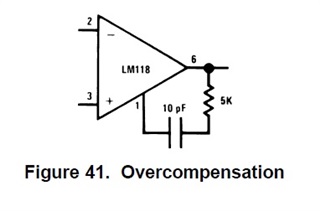
Figure 41 in the datasheet has a similar diagram, but our board does not have a 5kΩ resistor.
(Incidentally, please tell me what the purpose of the circuit in Figure 41 is.)
If you can guess the design intent, please let me know.
Best regards,.
Nobita
Hello kai
Thank you for your reply.
Our circuit is a little different from the diagram you presented.
That circuit only has a 10pF capacitor placed between pin 1 and pin 6 (instead of pin 8). In that case, is there any effect in improving the settling time?
Best regards,.
Nobita
Hello Nobita,
The BAL/COMP1 node is inverting relative to output. The capacitor is used to lower the gain bandwidth product.
What is the of the LM318 stage schematic in your design?
Hello Ron
Thank you for your reply.
Our circuit consists of two stages of inverting amplifier circuits using LM318.
A 10pF capacitor is connected between the 1pin and 6pin of the operational amplifier for both the first and second stages.
Is this answer what you expected?
Best regards,.
Nobita