This thread has been locked.

If you have a related question, please click the "Ask a related question" button in the top right corner. The newly created question will be automatically linked to this question.

XTR111: Designing with XTR111AIDRCT

Part Number: XTR111
Other Parts Discussed in Thread: XTR300, XTR305, OPA192, OPA197, OPA202, TMUX6219

Hello Team,
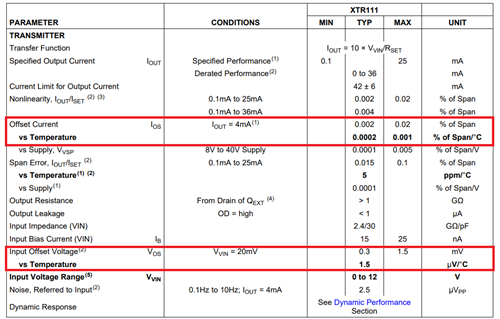
I am planning to use XTR111AIDRCT for one of our products to get a 4-20mA output current corresponding to a sensor output.
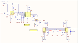
The 4-20mA output current will be fed to a connector.
A 0-10V analog output voltage shall be provided to the same connector.
A GUI can decide the voltage or current output at the output connector.
When analog voltage is needed at the output connector, the current output will be disabled.
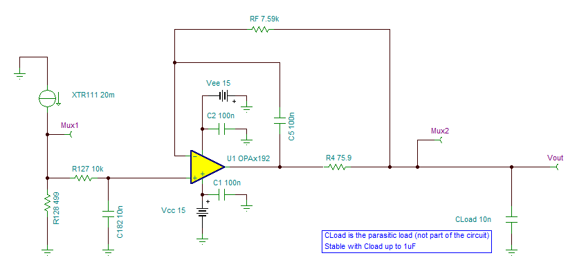
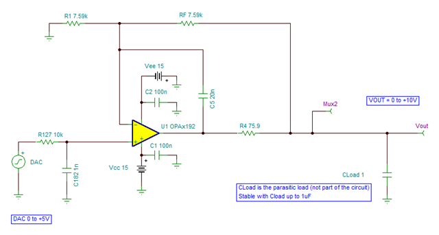
I am planning to design my circuit as follows.

A shunt resistor (249 Ohms) will convert the 4-20mA to 0-10V.
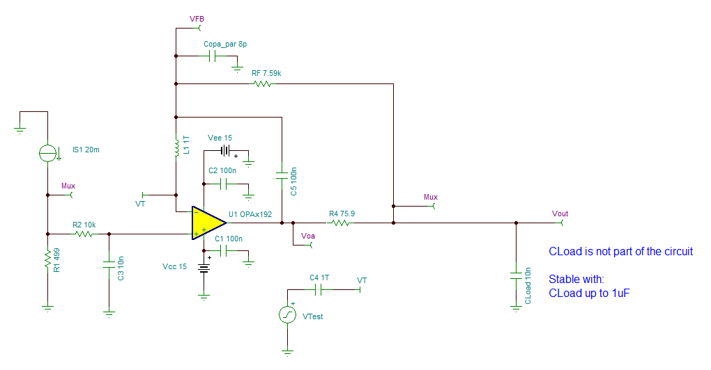
Since the XTR111 cannot generate a 4mA for a 0V input voltage at the VIN pin, we are planning to provide a certain voltage at the VIN pin from the DAC.
To get 0V the current must be 0mA.
What will the output current be if the input voltage at the VIN is 0V?

Looking forward for your response.

  • Hi Shibin,

    The error in output current due to the XTR111 device is dependent on the current offset, IOS, the internal amplifier input offset voltage, VOS, and the XTR111 Span error.  When VIN=0V, the span error does not play a significant role, and the XTR111 errors are dominated by IOS and VOS.  You will also need to account for any leakages due to external components such as protection diodes, and any errors due to the source circuit or DAC generating the input voltage applied to the XTR111.


    To provide an estimate (when VIN=0, and XTR111 output is enabled):

    - The XTR111 IOS current offset is 0.02% (max) of span at 25C, where span is specified to 25 mA.  Hence, IOS error is 25 mA*0.02% = ±5 μA max at 25C.

    - The XTR111 VOS input offset voltage is ±1.5-mV (max) at 25C. The voltage offset also translates into an output current error, depending on the RSET resistor value.  For example, if RSET is 2 kΩ, the current output is given by the relation IOUT = 10*( VIN / 2 kΩ). Therefore, the VOS= ±1.5 mV input offset voltage will create an additional current offset error of ~ ±7.5 μA at 25C when using RSET=2 kΩ. 

    -  In this example, the estimate of the output current error at room temperature, 25 C, would be approximately 5 μA + 7.5μA  = ±12.5μA when using RSET = 2 kΩ. 

    Please note, this estimate does not account for additional leakage currents present in the hardware due to external protection diodes, or additional voltage offsets errors external to the XTR111, for example, errors due to the DAC generating the input voltage.  Also, the temperature drift of IOS and VOS needs to be accounted as well as the device temperature changes.

    When output is disabled with OD = high, the XTR111 typical leakage current is ~1µA.  This specification does not include errors due to leakage due to external protection diodes or external components in the current output module hardware.

    Thank you and Regards,

    Luis

  • Hello Team,
    Attached is the design of the Current/Voltage output circuit using XTR111.
    Please share your comments.


    The VIN pin of the XTR111 is driven from a 0-5V DAC output through a buffer.
    The 2*mux is used to switch between current output and voltage output.


  • HI Shiblin,

    - The XTR111 is a current output transmitter. On the multiplexer circuit above, when selecting the RLOAD = 249Ω, the resulting output voltage will change with any additional load impedance or resistance applied at the output of MUX  U38.  Essentially the XTR111 is providing a current output signal, and the output voltage will change as a function of the effective load combination of 249-Ω in parallel with the external load at the mux output since the voltage is not buffered. Is this the function that is intended?  

    The XTR300 and XTR305 are output transmitted/driver devices can be configured as current or voltage output mode that may be of interest.  The XTR300 and XTR305 share the same pinout.  There is a couple of reference designs with the XTR300 and XTRT305 below:

    - The XTR111 input signal is generated with the OPA192 powered with bipolar ±15V supplies.  This works, but a suggestion is to change R119 to 10-kΩ at VIN to protect the XTR111 input for the case of an unintended fault, where the OPA192 output may produce a negative voltage that could damage the XTR111 VIN input.

    - Choose a P-FET transistor in a package and thermal characteristics to support your max power condition without overheating, per the max supply and max output current requirements in the application. See a previous E2E thread below discussing the external PFET selection and optimal heatsink on the PCB layout.

    https://e2e.ti.com/support/amplifiers-group/amplifiers/f/amplifiers-forum/1206545/xtr111-2evm-output-mosfet-selection?tisearch=e2e-sitesearch&keymatch=xtr111%252525252525252520current#

    Thank you and Regards,

    Luis 

  • Hello Luis,
    Thank you for your reply.
    If I buffer the voltage generated across the 249Ω resistor, the load resistance at the output of the mux U38 will have no effect.
    But since I need a 0-10V analog output signal and a 4-20mA signal at the same terminal (selection by GUI), the opamp used for the buffer may not be able to drive high capacitance of the cable (as per the discussion on the link).

     XTR300 and XTR305 are not available on Mouser or Digikey or in TI Store.

    Do we have any other solutions to get a 0-10V industrial standard output?

  • Hi Shibin,

    You could use a OPA192 buffer in the dual feedback configuration.  On your circuit above, on the voltage output path, add the OPA192 buffer on the dual feedback configuration below, prior the second output multiplexer U38. This circuit is stable driving a capacitive load up to 1µF.

    Thank you and Regards,

    Luis 

    Circuit:

    Stability Analysis for Cload in the range of 100pF to 1uF:

  • HI Shibin,

    You could also modify the op-amp circuit for non-inverting gain of +2-V/V.  In this case, you could feed the 0-5V DAC output directly into the OPA192 (or OPA197 circuit) and generate a 0-10V signal.

    See below circuit for 0 to +5V DAC input and 0 to +10V analog output signal.   This circuit is also stable with 103-degrees of phase margin with 1nF load, and 115-degrees of phase margin with 1uF load.  I did not include the mux at the output in the simplified diagram below.  Keep in mind that a clamp circuit, TVS diode, is required at the output of the multiplexer.

    Thank you and Regards,

    Luis

  • Hello Luis,

    Thank you for your reply.

    Can I use op amp like OPA202IDBVR.

    This op amp is able to drive upto 25nF and if using Riso, it can be used to drive upto 100nF.

    I can use the dual feedback approach if I need to drive a capacitance of 1uF.

    Or am I missing something?

    Expecting effective capacitance of 100pF per meter, a 25nF capacitance drive will suffice.

    Also, any resistive load at the cable will form a voltage divider using Riso.

  • Also, any resistive load at the cable will form a voltage divider using Riso.

    No, the isolation resistor R4 of Luis's circuit is within the feedback loop and the voltage drop across it is compensated by the feedback.

    Kai

  • HI Shibin,

    If you wish to use the OPA202, this amplifier can work on this application.  The dual feedback configuration has an advantage, it eliminates any voltage errors on the RISO resistor when loading the circuit, in other words, eliminates the voltage output error due to the I*R voltage drop across the RISO resistor, so this is a good configuration for this application as a industrial voltage driver. Keep in mind, the suggested dual feedback configuration/compensation components need to always be adjusted per the specific op-amp GBW/Zo specifications and the capacitive load requirements.

    I see you have another E2E thread discussion.  Kai has suggested the circuit below which is quite stable with 96-degrees of phase margin up to 77nF.  It also is quite stable at 100nF.  However, without adjusting the circuit, ensure to limit the capacitance to less than 100nF, since a complex zero/pole forms causing an abrupt change in the loop-gain magnitude and phase when you apply capacitive loads much larger than 100nF in this circuit.

    As it has been explained on the other thread, the OPAx202 circuit is quite stable at 75nF, which exceeds your 25nF requirement.  Please limit the load capacitance to <100nF. This circuit is a good suggestion for your application.

    Thank you and Regards,

    Luis

  • Hello Team,
    Attached are the schematics of the analog voltage/current output using XTR111.
    Please review the schematic and share your comments.


    1). At some point during the operation, the inputs of the Opamp U23 (OPA192ID) or U40 (OPA202IDBVR) can be floating.
    Are there any issues with floating the input of the opamp?
    Now I am using a 100K resistor to prevent floating the input pins of the opamp.

    2). The DAC will be generating a voltage from 0V to 5V. I hope the TS5A4624DCKR is able to switch these low voltages from input to output.
    Please correct me if I am wrong


  • HI Shiblin,

    The TMUX6219 is powered with bipolar ±15V supplies.  You will need to add protection to the multiplexer output since it is exposed to the external connector.  During a fault, the output of the multiplexer can withstand an absolute maximum/minimum voltage of VSS-0.5V to VDD+0.5V or ±15.5V. 

    At the output of the TMUX6219, you have a bipolar TVS diode SMAJ40CA, which has a breakdown voltage above 40V, and will not protect the multiplexer.  If your application will only require to support unipolar output voltages from 0 to +10V, please consider replacing the TVS diode with the unipolar SMAJ12A with reverse standoff of 12V, and a breakdown voltage of 14.9V, and clamping voltage of 19.9V.  Also, since this is the first circuit that is exposed to the external connector, please add the Schottky diodes at the mux output going to the supplies, and use a small series resistor to limit current through the Schottky diodes.  Also, please add TVS diodes to the bipolar ±15V supplies to ensure they hold the voltage during a fault condition. A possible circuit is below:

    Regarding your questions:

    1)  As you have mentioned, the schematic includes the 100kOhm pull down resistors at the input of the op-amps, so the inputs are not floating. This will work.

    2) The TS5A4624DCKR specifies an input range from 0V to V+ supply (or +5V).  

    Thank you and Regards,

    Luis

  • Hello Luis, 
    Thank you for your reply.
    The user guide of the XTR111 recommends using a bipolar TVS diode (MPN - SMAJ40CA).
    The same output terminal act as the analog voltage/analog current output.
    So for 4-20mA output, the voltage can be more than 10V but not definitely 40V
    So the output of the mux can be above 10V.

  • Hi Shibin,

    according to section 2.2.1 of the user's guide supply voltages up to +44V can be applied to the EVM. Then the SMAJ40CA is a good choice. A bipolar TVS also makes sense since Q3 can withstand some negative drain voltage. But in your case with U39 at the output powered by +/-15V the SMAJ40CA is not suited. U39 gets toasted before the SMAJ40CA turns-on.

    And the unipolar TVS Luis has suggested also absolutely makes sense at an industrial 0...10V voltage output, since many process control inputs don't like all too negative going voltages at their 0...10V inputs at all. So, clamping the negative output voltage to one diode's forward voltage drop is a very good idea.

    I also have suggested an unipolar TVS in the neighbour thread, by the way:

    https://e2e.ti.com/support/amplifiers-group/amplifiers/f/amplifiers-forum/1213983/opa990-designing-with-opa990sidbvr

    Keep in mind that an EVM is an evaluation module and not a ready circuit. An EVM allows some changes to test the chip of question under varying conditions. From this point of view the SMAJ40CA makes sense. But you must not think that it is a ready circuit which you can copy and paste one to one into your circuit.

    Kai

  • Thank you Kai and Shibin,

    Kind Regards,

    Luis