Because of the holidays, TI E2E™ design support forum responses will be delayed from Dec. 25 through Jan. 2. Thank you for your patience.

This thread has been locked.

If you have a related question, please click the "Ask a related question" button in the top right corner. The newly created question will be automatically linked to this question.

LM675: Crossover distortion with loads below 100 Ohms

Part Number: LM675
Other Parts Discussed in Thread: OPA548, LM1875

Playing with the output snubber, I was able to remove most of the distortion in this circuit with loads below 100 Ohms (no distortion is visible with larger loads).

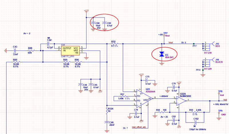
I removed the current sense amplifier and the output protection diode to ensure that they were not contributing. The present lowest distortion 'sweet spot' for this example is 10 Ohms (R124) and 4.7nF (C46). The originally recommended 1 Ohm 0.22uF snubber performs worse than no snubber at all. The feedback network doesn't affect these distortions. The resistive load was created with a scope 50 Ohm input termination and with a decade resistance box with the same result. Removing the scope connection (but retaining the resistive load) does not change the waveform (as viewed with a separate 10:1 probe).
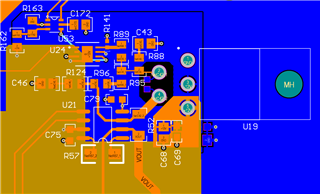
The source signal shows no such distortion (at R89). Any capacitance placed at C42 only adds ringing at the disconinuity.

I have several examples of this board with no such distortion, so it seems to be related to open loop gain variation between samples of the LM675 (which I would expect to be greater than 20dB, per the datasheet).

The power supply rails at the IC are perfectly quiet at the crossover distortion ponts (in time).

This is a part we were forced to use because the preferred OPA548 was unavailable.

Thank you, in advance, for your help!

  • Hi Michael,

    the purpose of the snubber at the output of LM675 is to increase the stability when connecting critical loads to the output of LM675 which may shift the phase within the feedback loop and erode the phase margin. The Boucherot or Zobel snubber decreases the open loop gain of LM675 by introducing a voltage divider which only acts above a certain frequency set by the time constant of snubber. The ohmic resistance in combination with the open loop output impedance of LM675 gives this voltage division.

    Because the snubber decreases the open loop gain and by this degrades the linearizing effect of feedback loop, it's no surprise that the distortion decreases when replacing the snubber by a milder one or even removing it all the way.

    I see an issue with C42. The LM675 is decompensated amplifier and needs a gain of more than 10V/V. C42 decreases the gain at high frequencies and may destabilize the LM675. Ok, 4.7pF is not very much and may still be uncritical. But keep it in mind when you intend to increase C42. I wouldn't do that.

    And there's another issue with R88 and C43. The idea of this network is to increase the noise gain to above 10V/V (above a certain frequency set by the time constant of R88 and C43), if the overall set gain of LM675 is lower than 10V/V. But with the components you have chosen the noise noise gain is way higher, namely 36V/V. So, you have less linearizing gain reserve of LM675, increasing the distortion. I would try to increase R88 in small steps up to 2k2 or so and adjust C43 accordingly.

    Kai

  • Hi Kai,

    Using the open loop response curve in the LM1875 datasheet (which other TI engineers have claimed is quite similar to the LM675), I tampered with an existing LM1875 model to produce a phase/gain profile more like the graph shown in the LM1875 datasheet.

    This revealed that my lag circuit (R88/C43) needed to have a relatively low corner frequency to avoid phase margin degradation at the 0 dB crossover frequency. R604 was adjusted to trim the crossover frequency. The relatively low second pole in the amplifier itself forced me to push the stable crossover frequency downward to avoid the second pole's cumulative phase shift.

    Unfortunately, the model still doesn't represent the rising-output-impedance-with-frequency characteristic which the Zobel snubber exploits, so I'm back to physical experiments to work with that circuit.

    Thank you for your help!
  • Hi Michael,

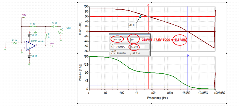
    a gain bandwidth product of 5.5MHz is not very much when you want to handle 100kHz at a noise gain of 36V/V. This gives a gain reserve of only 1.5V/V. I think you cannot expect a lower distortion with this low gain reserve.

    Kai

  • Hi Michael again,

    have you thought about using the LM675 as a non-inverting amplifier with a gain of 10V/V? You could mount a voltage divider at the +input of LM657, if you don't need the whole gain. And if you need a signal inversion you could add an inverting OPAmp with a gain of -1V/V in front of the LM675. This would allow you to get rid of the R44/C43 compensation network and to profit from a higher linearizing gain reserve Relaxed

    Kai

  • Hi Kai,

    Thank you for the suggestion! This product is a power function generator, so while we have been using uP DC calibration to tweak the 20mV offset uncertainly with 2X DC gain,this becomes less trustworthy with 100mV. I was thinking of trying this just to see if it really helped with the noise, though. All my previous feedback path experiments had no effect on this noise; as if the full open loop path through the amplifier was too slow to deal with this step in the amplifiers output stage (under significant load).

    Thank you for your help!
  • Hi Michael,

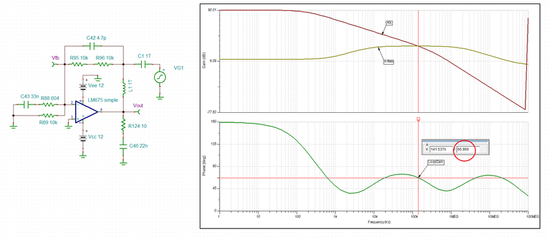
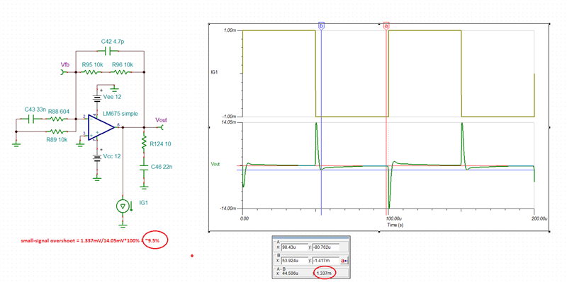
    I have created a crude macro-model for LM675 with the limited info available (no plot of AOL vs frequency) - see below.

    Using the model I find that at the intersection of AOL and 1/beta the gain is set by the ratio of 20k and 604 resistors resulting in effective gain of 33.  Thus, the circuit seems pretty stable with phase margin of 67 degrees - see below.

    Transient simulation confirms its stability with the small-signal overshoot of less than 10% - see below. 

    Since LM675 its a bipolar output amplifier, I have assumed resistive output impedance of 10ohm. Its DC value may be closer to 1.5ohm allowing 4V swing under 2.6A load - see datasheet for output voltage swing conditions (21V/8ohm).  Lower output resistance improves stability. 

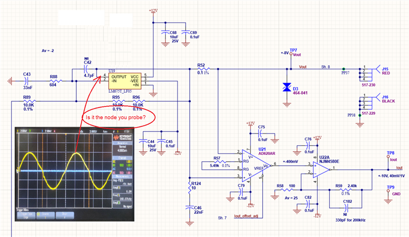
    As far as the cause of the distortion, I wonder where exactly you connect the scope probe? (I do not see TP directly at the output of LM675)

    Michael LM675 AC stability.TSC

    Michael LM675 Transient stability.TSC

  • Hi Marek,

    Thank you for your modeling work!

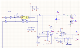
    This is the modified subcircuit I am using. It was created by editing a model I found of the LM1875 which was, according to a past TI e2e contributor, similar to the LM675. Most of the effort involved adjusting the second pole to provide phase/gain results more like my oscillating boards.

    lm675LTSPICEsubckt.txt
    *-----------------------------------------------------------------------------
    * connections: non-inverting input
    * | inverting input
    * | | positive power supply
    * | | | negative power supply
    * | | | | output
    * | | | | |
    .subckt lm675 1 2 3 4 5
    *
    * Modified 4/13/2023 by M.Henderson to match LM675 datasheet A*beta response
    *
    * c1 11 12 8.660E-12 (original value)
    c1 11 12 40.00E-12
    * c2 6 7 15.00E-12 (original)
    c2 6 7 6.00E-12
    dc 5 53 dx
    de 54 5 dx
    dlp 90 91 dx
    dln 92 90 dx
    dp 4 3 dx
    egnd 99 0 poly(2),(3,0),(4,0) 0 .5 .5
    fb 7 99 poly(5) vb vc ve vlp vln 0 7.717E9 -7E9 7E9 7E9 -7E9
    ga 6 0 11 12 518.4E-6
    gcm 0 6 10 99 16.40E-9
    iee 3 10 dc 120.4E-6
    hlim 90 0 vlim 1K
    q1 11 2 13 qx
    q2 12 1 14 qx
    r2 6 9 100.0E3
    rc1 4 11 1.929E3
    rc2 4 12 1.929E3
    re1 13 10 1.493E3
    re2 14 10 1.493E3
    ree 10 99 1.661E6
    ro1 8 5 50.00E-3
    ro2 7 99 50.00E-3
    rp 3 4 2.796E3
    vb 9 0 dc 0
    vc 3 53 dc 4
    ve 54 4 dc 4
    vlim 7 8 dc 0
    vlp 91 0 dc 3.000E3
    vln 0 92 dc 3.000E3
    .model dx D(Is=800.0E-18)
    .model qx PNP(Is=800.0E-18 Bf=300)
    .ends
    *$

    With loads over 100 Ohms, this seems to be a reasonable representation of my observations.

    However, as my loads drop below 100 Ohms, different forms of oscillation arise in the actual circuit which do not occur in the SPICE simulation.

    Outside of a 100mOhm output R (50m as a shunt R + 50m as a series R), this model does not seem to model the increasing output impedance one would look for in a model susceptible to influence by a Zobel damper with a 1 to 10 Ohm resistive element.

    This would explain the lack of my SPICE circuit performance dependence on the Zobel snubber; even at 1 Ohm, it is large compared to these small open loop source R's.

    I also note the internal offset between two virtual grounds, equal to the difference between one half of each power supply. This comes to 2V (20V/2 - 16V/2) and does appear to be an output amplitude threshold beyond which my real circuit misbehaves more.

    I think I need to do more modeling in the time domain with sine/triangle waveforms to look for better correlation, although the fixed open loop output Z appears to be a continuing problem.

    Thank you for your help!
  • Here is an image of my SPICE schematic with the above LM675 model:

    This site won't let me upload the actual .asc file.

  • Michael,

    I doubt that the distortion you see is caused by questionable stability of the circuit. Could you confirm the node you show as distorted?  If it's a different one than shown below, please specify which node you probe.

  • Hi Marek,

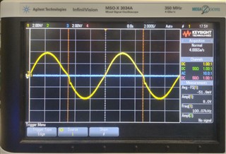
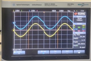
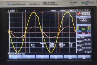
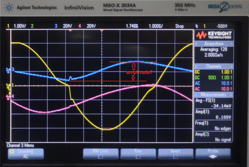
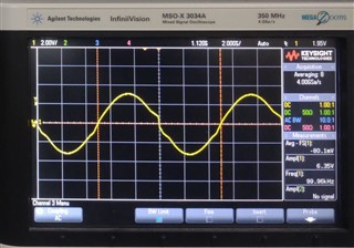
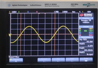
    I see the same distortion at U19 pin 4 that I see at J15 (they are only 0.1 Ohm apart). Here's a picture of both from a different board (with the same issue and output path):

    This is with a 50 Ohm load. As I go above 2V peak, oscillation starts in the top half of the waveform.

    Thank you for your help!

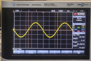
  • Michael,

    This does not look like oscillation but rather a distortion.  Could you slow down the frequency by 2x to 50kHz and see if there is any decrease in distortion?  

  • Hi Marek,

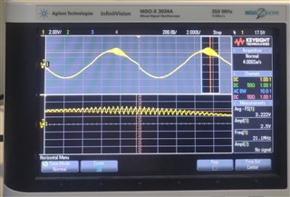
    Here's a image with a signal above 2V peak, which results in top half oscillation (about 20MHz in this case). 

    This is also reduced by increasing load R to 70 Ohms or higher.

    I'm playing with Zobel values now, but I'm thinking that this network may need to change as my external load changes; problematic for a function generator.

    Thank you for your help!

  • I just discovered that our original design with the OPA548 displays the same distortion:

    The bandwidth on this part is lower, which is reflected in the 'softer' corners of the distortion step.

    The original design also uses asymmetric supplies, so that may be an issue for amplifiers.

  • Michael,

    This definitely looks like oscillation.  Could you verify that you do have bypass caps on +12V supply pin?  Also, could you disconnect the bidirectional TVS (D3) to see if it makes a difference - see below.

  • Hi Marek,

    Yes, the power supply capacitors are there. I even added a cap to the negative rail when I saw 5mVpp of correlated (the the glitch) noise on the negative rail to reduce this noise with no effect on the glitch in the output waveform. Removing D3 has no effect. Removing U21 has no effect.

    I will spend the rest of the day looking at bandwidth reducing measures that also increase stability.

    Thank you for your help!

  • Changing to DC gain of 20 with no lag compensation and 1 to 5 Ohm Zobel R with 0.18uF Zobel C eliminates oscillations at all amplitudes and frequencies, but transient is more apparent (but still a single 'step' without ringing).

    I will play more with Zobel values tomorrow and try increasing feedback network impedance to see if that reduces output transient bandwidth. Signal bandwidth meets goals right now (<6dB down at 200K, <2dB down at 100kHz).

  • Using 100K/10K feedback network without lag network (wideband gain of -10) and 4.75 OHm/0.18uF Zobel snubber, no oscillations are seen; only the 'step' transient, which does not vary much with the amplitude of the output sine wave:

    These were both taken with a 50 Ohm load.

    As the load resistance is varied from 10 Ohms upward, the 'step' moves in phase relative to the sine wave.

  • Michael,

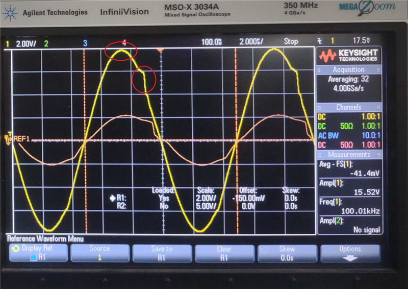
    I still see a small-signal oscillation and large distortion - see below.

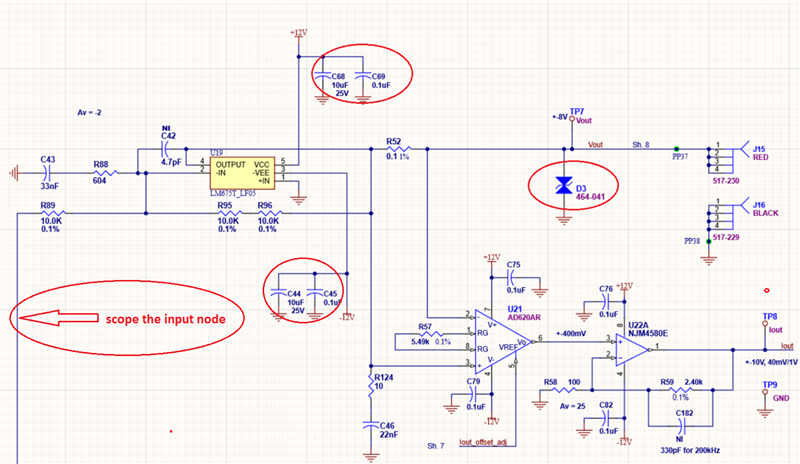
    Just for sanity check, could you scope the input signal - see below.

  • Hi Marek,

    Here are some captures. There is no noise at the top of the previously posted output waveform. You have circled the digitization quantum step of the scope. The waveforms below were cleaned up by averaging, but I looked at them un-averaged first to ensure no high frequency uncorrelated oscillation was being hidden.

    850 Vout, 100k/10k Rfb/Rin 4.7/0.1u Zobel w/Vin (blue) and high Z load:

    850 Vout, 100k/10k Rfb/Rin 4.7/0.1u Zobel ckt, +12V(red) & -12V(blue) Rails with high Z load:

    This was with an extra 22uF added at the -12V Vee pin of the amp to gnd, which reduced noise around the transient step from 50 to 3mV, but had no effect on the output transient shape or amplitude. The abrupt change in slope of Vee seems to indicate that some portion of the output stage simply stops drawing current around the time of the transient, as if the sourcing and sinking transistors are not overlapping in conduction.

    I'm using high-Z loads to minimize the effects of power supply noise on the (unchanged) output distortion.

    The lack of step noise dependence on the beta network and input amplitude leads me to believe that this is related to the final stages of the amplifer. 

    I have stopped removing the output protection diode, as doing so does not change the transient size or shape.

    Thank you for your help!

  • Hi Michael,

    Some other possible cause of distortion occurred to me.  Just to be sure, you still use +/-12V supplies and the output voltage is +/-4Vp or 8Vpp, correct? 

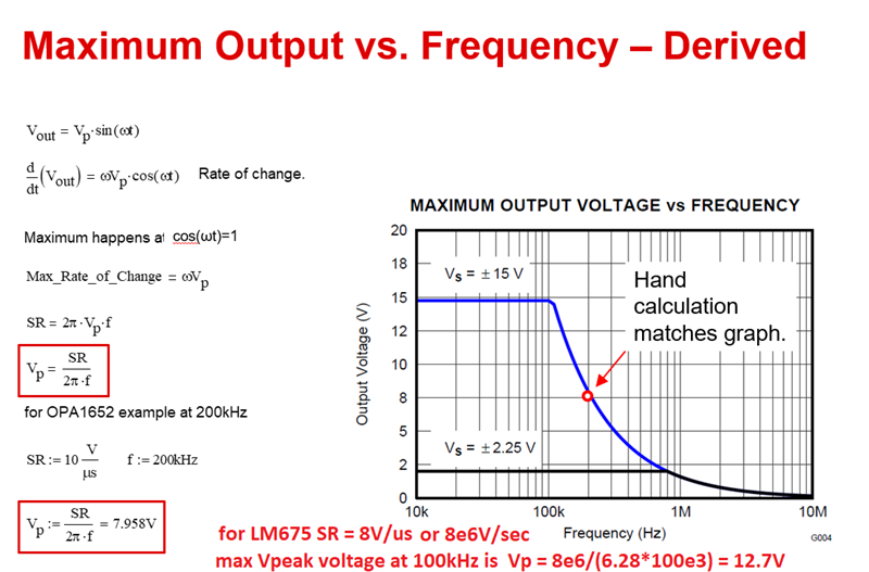
    For a large input/output voltage (e.g. G=1), the maximum output voltage vs frequency is a function of slew rate (SR) - see below.  Thus, at 100kHz input signal, the maximum peak output voltage (Vp) can be calculated to be 12.7V (see below) and above said voltage the output will be distorted by slew limitation - in other words, the input frequency would be too fast for the output to keep up.

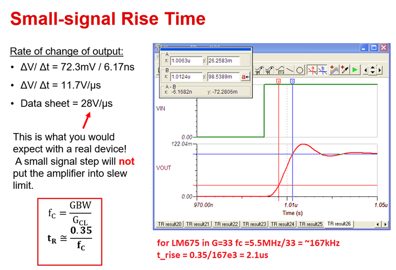
    However, as I simulated it previously, at 100kHz the gain is determine by the ratio of 20k and 604 resistors resulting in effective gain of 33. This means that for the output to have Vp=4V, the input signal magnitude must be around of 121mV - this is a relatively small signal where the input signal magnitude is not high enough for the output to slew.  Under such conditions the output response is controlled by the Small-signal Rise Time instead of slew and in the case of LM675 one-time constant settling time may be calculated to be around 2.1us - see below.  This means that at 100kHz where output signal must travel 8V within 5us, the output can settle only to within 5us/2,1ua= 2.38 time-constants or 1-exp^(-2.1) = ~91% resulting in output distortion. 

    All in all, a lowering of the input frequency or the magnitude of the input/output signal should solve the distortion issue.

  • Hi Marek,

    While slew rate limiting is expected and seen, our two products which use this amplifier (one with +/-12V rails and one with +20/-16V rails) both display this 'notch' visualized above. I was able to reproduce the problem with our older products which utilize our original OPA548, although the distortion is smaller.

    Thank you for your help!

  • Michael,

    Slew limiting (discussed in the first case above) applies ONLY if the input signal amplitude is 1V or higher.  For the small input magnitude like 121mV, op amps will NOT slew but instead will respond according to the small-signal rise time formula shown in the second case above. 

    Because of its much lower GBW of 1MHz, OPA548 small-signal rise time is 11.55us - longer than a period of 100kHz signal.  Thus, I would expect a significant distortion seen at the output.

    All in all, I think it would be really useful at this point to either lower the amplitude or frequency of the input signal by a factor of 2 and see if this removes or at least diminish the distortion you see.

  • Hi Marek,

    As I vary the sine wave amplitude and frequency of the input to these amplifiers, the crossover-like 'notch' distortions referred to above change relatively little. Unlike slew rate limiting distortion, these 'notch' events are characterized by slew rates that are faster than intended, not slower. Also, the distortions I see vary in phase relative to the sine waves they are superimposed on as load reactance varies, but not in shape. This is nothing like the internal gain stage based slew rate limiting you seem to be referring to.

    Next, I will be trying bias currents to power supply rails, although this will probably just offset the distortion events.

    Thank you for your help!

  • Hi Michael,

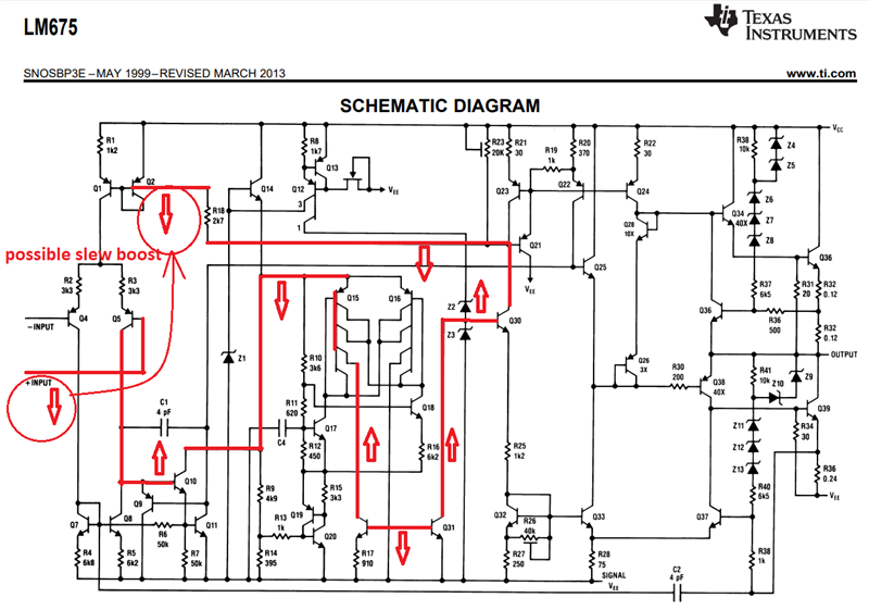
    LM675 comes from TI acquisition of NATIONAL SEMICONDUCTORS, thus I'm not sure if this is the case BUT I could think of one more possible explanation for the distortion you see - a slew boost.  Slew boost detects a large differential voltage between the input terminals and in response increases the tail current (look on schematic for Q1) biasing the input differential pair - this in turn increases the slew rate, which is a function of the tail current: SR=Itail/Cc where Cc is a Miller compensation cap. If this in fact is the case, for frequencies between the natural (unboosted) and boosted full-power bandwidth, the op amp may switch between the boosted and upboosted slew resulting in the distortion you see. 

    Looking at the simplified schematic of LM675 I see a signal path of a possible implementation of the slew boost - see below.

    Below please see the presentation discussing topic of slew rate.

    Slew Rate_Updated_01.pptx

  • Hi Marek,

    Thank you for the schematic and powerpoint!

    This is the first I have seen of a LM675 schematic, which differs a bit from the LM1875 schematic I had been referred to (especially regarding the net which includes the junction between two Zener diodes).

    SInce I have wired the circuit with 10 to 30X DC gain and wired it with 2X DC gain (with the added lag circuit) while adjusting input voltage to attain a given output voltage (8Vpp Vout is a routine test value) without correcting this issue, I would say this is not something which disappears with decreasing input voltage.

    I can say that the crossover distortion appears when loads become 'heavier':

    This is the +/-12V circuit with a DC gain of 2, a high frequency gain of 33, 10 Ohm/4.7nF Zobel network, and 10 Ohm (orange) versus 200 Ohm (yellow) DC loads. 

    How would the internal slew rate correction loop you describe be influenced so much by the output load resistance?

    Thank you for your help!

  • Hi Marek,

    The OPA548 version (older design, source restricted), shows much less crossover distortion. Might you have a schematic for this part? It isn't in the datasheet available to me.

    Thank you for your help!

  • The slew boost changes the gm of the input stage and thus effects overall compensation of the circuit.  However, as Kai previously wrote the cause of the distortion may come down to the fact that the snubber decreases the open loop gain and by extension degrades the linearizing effect of feedback loop especially under heavy load conditions changing effective output impedance, Zo. This may be confirmed by decrease in distortion under milder snubber.  Therefore, it may be useful to remove the snubber all together and see if there is any distortion left under heavy purely resistive load.

  • Hi Marek,

    Running without the output snubber and a low Z load (say, 50 Ohms) produces oscillation, especially during the top half of output waveforms (say, a sine wave at 1 to 100 kHz).

    Running with a 1 Ohm/0.2uF output snubber and high Z loads (100 Ohms or greater) produces oscillation.

    Thank you for your help!

  • Hi Marek,

    Here is a view of the circuit with a 100kHz sine wave source, a 10 Ohm load, 332 Ohms R88, 20nF C43, 10 Ohms R124, and 22nF C46:

    The largest ripple here is 40mVpp and the Vee (blue trace) noise around the cross-over glitch is about 4mV.

    Is this noise large enough to be problematic? Adding more C's to this rail I can halve this noise without apparent changes to the crossover glitch.

    This is the best combo I have found, given the present topology. Increasing DC gain to 10 or even 30 (while eliminating the lag compensation) does not influence this crossover glitch.

    We are looking at going back to the OPA548, which will be another costly board turn, since that part is available again.

    Thank you for your help!

  • Michael,

    I'm not sure I follow the scope waveforms below - other than noise, does Vee (blue trace) value changes and if so what's the amplitude?  I thought your supplies are constant +/-12V - please explain?  Also, please identify remaining traces.

  • Hi Marek,

    The blue trace is Vee (-12V feeding the amplifier negative power supply pin) and the pink trace is Vcc (+12V feeding the amplifer positive power supply pin).

    The yellow trace is Vout.

    The voltage scale is listed for each of the three waveform colors.

    The Vee waveform shown is about 26mVpp with a transient of roughly 4mV associated with the crossover transient.

    The Vcc waveform shown is about 40mVpp with a barely perceptible transient associated with the larger crossover transient.

    The Vee and Vcc traces are AC coupled and only document the noise associated with the output waveform.

    Lower output snubber capacitance increases ringing arount the crossover transient.

    Thank you for your help!

  • Michael,

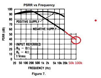
    Powers supplies should not be varying so much - at 100kHz PSRR is at best 40dB or less (see below - PSRR not shown above 20kHz). Now I begin to think that the issue may be with the trace inductance of the PCB or weak supplies. What is the ESR of the supply caps you use and how close are the caps to supply pins?  Any chance you can try a different (more robust) power supplies?

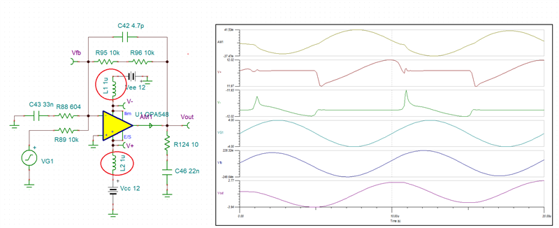
    I just simulated 1uH series inductance with OPA548 supply pins and notice a gross distortions - see below.  This could help explain why you see distortion (to various degree) with all of the op amp you try to use.

  • Hi Marek,

    40mV out of 12V is a ripple of 0.3%. Using your graph, this would be reflected in the output as 40mV/100= 0.4mV; a tiny fraction of the noise we see on the outputs. The negative supply noise is even smaller.

    My SPICE model includes 0.5 Ohms of power supply source resistance before my local (via copper pours within 0.25" inch of the amplifier) capacitors modeled in SPICE as 93n and 2.95u for each rail.

    The waveshapes shown in my last attachment indicate the capacitive nature of the supplies as seen at the leads of the amplifier (where the probes touched the nets). Note how my supply voltages start declining as soon as that rail starts to conduct current into the load (as indicated by the polarity of the output voltage relative to ground).

    This is quite unlike your model.

    Your current waveform (AM1) does look familiar in my output voltage shape and I will try re-routing  my output snubber to avoid sharing it with my feedback path (I didn't insist on segregating this path in my layout guidance).

    I will try piling on more bulk capacitance with focus on 100kHz impedance, but this doesn't address the crossover transient which is much higher in frequency and was already experimentally reduced with added caps (around 2uF). Despite reducing the crossover transient on the negative supply by a factor of 3, no change was seen in the output waveform transient.

    Thank you for your help!

    Mike Henderson

  • Sounds like a good plan.  Good luck!

  • Hi Marek,

    Quickly throwing a 22uF 25V 1210 ceramic cap with an SRF of roughly 1MHz from pin 1 to 3 of my LM675 (reducing my local Vee Z by 2/3's) didn't do much to my Vee ripple; still just under 20mV with no change in the crossover transient (which would be well into the inductive domain of the 22uF cap anyway). 100kHz 300mA pulses from my 10 Ohm load driven by 3V peak waveforms would make about 50mVpp at Vee, so I'm clearly getting some help from my 70+uF of ceramic capacitance distributed elsewhere on the PCB.

    Separately routing the output snubber directly to the output lead of the LM675 package had no effect. 100kHz 300mA pulses would make about 50mVpp at Vee, so I'm clearly getting some help from my 70+uF of ceramic capacitance distributed elsewhere on the PCB.

    Thank you for your help!

  • Hi Michael,

    please don't feel offended, but to me it looks a bit as if you are beating a dead horse. You run a 5.5MHz OPAmp with a noise gain of 36V/V at a frequency of 100kHz resulting in a linearizing gain reserve (loop gain) of only 1.5V/V. And the Zobel network even decreases this gain reserve. Sorry, but you cannot expect a distortion free performance with this circuit. When changing the Zobel network and the load you will get an endless series of different distortion patterns. But you will not find a solution without any distortion. This is impossible because you don't have any sufficient linearizing gain reserve. You may only achieve marginal improvements. But the main problem, the absence of sufficient linearizing feedback persists.

    You can either decrease the noise gain by increasing R88 and accordingly decreasing C43 or by chosing a way faster OPAmp.

    Kai

  • Hi Kal,

    Thank you for your appraisal!

    I have run this (LM675) amp with a DC gain of 10 with no lag compensation (about the lowest gain I think this thing can stand) and still see obvious distortion:

    Here is our (supply shorted) OPA548 waveform with the same frequency, amplitude, and 10 Ohm load:

    The 548 solution was set to a wideband gain of 1.5 with the default 1 Ohm 0.2uF Zobel snubber. The 6x lower feedback attenuation is certainly helpful for crossover distortion reduction, but the GBW of the 548 is also 1/5th that of the 675, which I was hoping would compensate. Since the 675 datasheet lacks an open loop graph, I had to guess at the gain at my high frequencies.

    It looks like we will be discarding the 675 part. Now I know why they are so available!

    Thank you for all your help!

    Mike Henderson