This thread has been locked.

If you have a related question, please click the "Ask a related question" button in the top right corner. The newly created question will be automatically linked to this question.

INA849: INA not working practically as per datasheet in theory

Part Number: INA849
Other Parts Discussed in Thread: INA848, , INAEVM-ALT-SO8

I have selected an INA848 IC instrumentation amplifier for a project for the following unique features observed in it’s datasheet that matches my requirement.
- Output Amplitude vs Freq graph - 0 to 5Vpp @500kHz with Power rails at +/-5V(Datasheet page 13)
Can go even from 0 to 12 Vpp @500k Hz with power rails at +/-15V
- Gain 1
- Slew Rate: 35V/us
- CMRR: 62dB @500kHz

The requirements I need for my project application are as follows:
- Input constant frequency: 500kHz
- Input Amplitude: 4 - 5 Vpp
- Ampifier Gain: Unity Gain (To have variable gain whenever needed)
- CMRR: Good
- Good Slew Rate

Datasheet: www.ti.com/.../i...15411&ref_url=https://www.google.com/

I have observed the following limitations in this IC when I test it practically on a breadboard.
- With power rails set at +/-5V, The output sine waveforms starts distorting at input of 2.5 Vpp @500kHz although the datasheet mentions that the output Vpp can go upto 5Vpp @500kHz
- When I test it using +/-15V power rails, the IC gets super hot and I feel that it wil burn off, so I’m guessing it would get defective when the IC gets super hot. It does not seem to match the datasheet. The datasheet mention on page 13 that at +/-15V power rails, at 500kHz the output can reach upto 12V pp but the IC starts getting super hot when I start increasing the the power rails from +/-5V

Please assist me. Is there something I am doing incorrectly during the test setup? I have checked my connection multiple times, but it always gives me the same results. Have tested it with two different ICs, both give the same results.

Any help would be highly appreciated.

  • HI Priyanka,

    I assume you are referring to the INA849 as shown on the title of the post, and INA848 in the description above is a typo, since you require gain=1V/V, and the INA848 has a fixed gain of 2000V/V.  Let me know if this is not the case.

    1)To ensure we understand your circuit, please post a complete schematic.  What is the reference pin voltage?

    2) This precision device can be tested on a custom PCB board with optimal board layout, or using the INA evaluation board. A suggestion may be to test the device using the INAEVM-ALT-SO8 evaluation module to simplify the setup and avoid potential issues related to the breadboard:

    INAEVM-ALT-SO8 — Evaluation module for instrumentation amplifiers with alternate pinout in SO-8 (D) package

    3) The post describes a signal amplitude of 4-5Vpp at 500-kHz.  What is the input common-mode voltage of the signal with respect to GND?

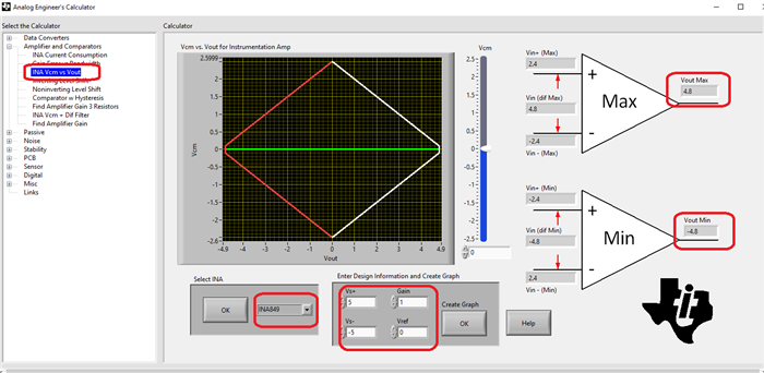
    The INA849 is an instrumentation amplifier. The maximum differential voltage that can be supported by the instrumentation amplifier depends on the input common-mode voltage, the V+, V- voltage supplies, the instrumentation amplifier gain, and the INA reference pin voltage. The "VCM vs Vout for Instrumentation amplifier" is a tool used to verify the instrumentation amplifier is within its linear region. The “Vcm vs. Vout” software tool considers the input and output limitation of each internal amplifier and displays a system level graph showing the linear output range as a function of input common-mode voltage.

    You may download the Analog Engineer's calculator in the link below and navigate to the "INA Vcm vs Vout tab" to check the INA849 input and output voltage range.  In the GUI, you need to input the voltage supplies, the reference voltage, the gain and the input common-mode voltage.  The calculator displays a plot of the vout voltage range vs input common-mode voltage agne. The "Help"  button on the "VCM vs Vout for instrumentation amplifier" tab provides a more detailed explanation.

    www.ti.com/.../ANALOG-ENGINEER-CALC

    As shown on the VCM vs Vout results below, the max and min output voltage supported is only±4.8V, when configuring the device with G=1V/V, VREF=0V, VCM-0V, and ±5V supplies.

    Thank you and Regards,

    Luis