This thread has been locked.

If you have a related question, please click the "Ask a related question" button in the top right corner. The newly created question will be automatically linked to this question.

OPA2192: How does input bias current change close to supply rails?

Part Number: OPA2192
Other Parts Discussed in Thread: OPA2196, OPA192, TINA-TI, ADS7046, ADS8860, OPA320, OPA328, OPA625

Hi,

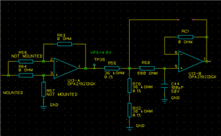
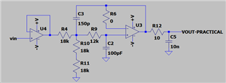
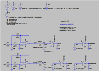
we have the above opamp configuration to measure the DC-link voltage in our frequency converter for maritime applications (800kW to 6MW power range). (Ahead of this circuit there is a high voltage voltage divider not shown). The opamp is powered from a single supply rail (GND to +15V). We want to be able to measure voltages close to 0V. I have selected the OPA2192 for its "beyond the rails" performance. (The voltage divider R56+R76+R112 is there for legacy reasons, we had a 5V ADC in the design previously). When I feed this circuit with 0V input, I measure 0.6mV at the output of the U13-A amplifier (buffer). At the output of the U13-B amplifier (filter), I get 19.3mV. This is quite a lot more than I expected. If I remove capacitors C43 and C44, I get 3.1mV at the output of U13-B. This is more in line with what I was expecting. The input bias current into U13-B.5 is supposed to be 5-20pA. At 20pA and 36k||72k=24k impedance it should be 0.48uV(?) Why is there less bias current with no capacitors?

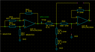
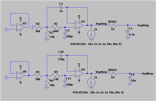
As an experiment, I did a redesign of the filter stage to lower the resistances like this:

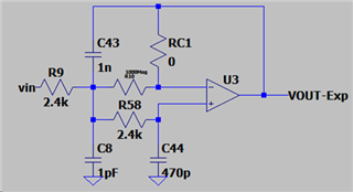
The result is that I get 0.8mV at the output of the buffer stage and 5.9mV at the output of the filter stage (success).

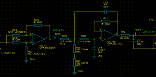
It seems that the bias current of the filter amplifier is something like this for my circuit and 0V input voltage:

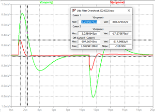
Original circuit: (19.3mV-0.6mV)/(24kohm+680ohm)=0.76uA

Modified (lower resistance) circuit: (5.9mV-0.8mV)/4.8kohm=1.062uA

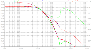
I see that you have a graph of the input bias current vs common mode voltage in figure 18 in the datasheet. The graph only shows the middle of the common mode range.

How does the input bias current change close to the negative rail?

(PS: We will probably change the design to use the OPA2196 due to availability and cost. I get similar results with that part as well)

  • Hello, thanks for your question.  

    1. I think the issue you are seeing is related to the output swing limitation.  The "beyond the rail" performance relates to the input common mode.  So, your 0V input on a 12V single supply operation does not violate the common mode requirements of the amplifier.  However, the output also has limitations with relation to the power supply (Voltage output swing from rail).  In the case of the OPA192, the output swing limitation is 15mV from the rail.  Thus, in the case of a single supply buffer with 0V input, the output is not valid until the input reaches 15mV.
    2. I/O Limits document is a document that covers this in detail.  Op amp video series has a section on input and output limits as well.
    3. Regarding output swing limitation:  All amplifiers have this limitation.  It can range from a few millivolts on CMOS amplifiers to volts on bipolar devices.
    4. One approach to solving the output swing limitation is to generate a small negative voltage for the amplifier negative supply.  Thus, the negative supply is -0.3V rather than 0V (GND).  Charge pump circuit (–0.3V) for negative amplifier supply illustrates this approach.
    5. Another approach that would allow you to measure down to zero volts input is to use a diff-amp configuration.  The reference pin on the diff-amp need to be connected to a positive voltage (e.g. 0.5V).  The output of a diff-amp is Vout = VinxGain +Vref.  So, if gain is 1V/V, Vout = Vin + Vref.  For a 0V input the output would be Vref.  Ideally you can connect the diff-amp output to a differential ADC input where the ADC measures between the amplifier output and the reference pin.  Below is a TINA circuit for a diff-amp using OPA192.  One disadvantage of a discrete diff-amp is that the resistor tolerance will impact accuracy.  Many applicatioins can tolerate this issue, but for higher accuracy you could use and integrated diff-amp like https://www.ti.com/lit/ds/symlink/ina597.pdf 
    6. To answer your question on bias current, it is relatively flat and very low for OPA192 across input signal (see figure 18).  I don't think bias current is the issue.

    diff amp opa192.TSC

    I hope this helps, Best regards, Art

  • Hi,

    I'll comment your inputs point by point:

    1. My first inclination was that the problem was output limitation. I removed R15 from the circuit so that the amplifier has no load. According to the datasheet, I should get a "typical" value of 5mV in this situation. Note that U13-A manages as low as 0.6mV into 108kohms. Both U13-A and U13-B are now operating at unity gain. The difference between the two circuits is that U13-A sees 0-ohm source resistance (I strapped it to GND) and U13-B sees about 24kohm source impedance plus some capacitors. If we assume that U13-B is for some reason performing far worse than U13-A, I should get 15mV at the output and not 19mV.

    2. Thanks for the document. I skimmed through it. Quite interesting but I did not find anything that would explain the behaviour I am seeing.

    3. I know

    4+5. This is the obvious solution. My board is in running series production. The 19mV is not really a big problem and we will live with it unless I find a simple fix that does not entail a new layout.

    6. Thanks for the clarification. I did not read the graph correctly.

    I still do not understand what I am seeing.

    Experiment 1: 

    Remove load and Remove feedback capacitor C43 (slightly simpler circuit). My circuit looks like this:

    I measure 19mV at U13-B.5 (and at U13-B.7). There is a very real DC current flowing through R58. How can this be explained by "output swing limitation"?

    Experiment 2:

    Remove filter capacitor C44. My circuit now looks like this:

    I measure 3.1mV at U13-B.7. This is in line with the datasheet value (5mV typical) into an open load. It seems that the presence of capacitor C44 mysteriously affects the DC-current through R56? (I am sorry but I did not measure U13-B.5 in this experiment. Confounded)

    Experiment 3: 

    Lower resistance of filter stage (keep frequency response close to original circuit). My circuit now looks like this:

    I measure 6.7mV at U13-B.7. The output from U13-A.1 is at 2.6mV so this is in line with the datasheet (2.6mV+5mV typical). This is the circuit I think I will go with on the next iteration of the BOM.

    Clearly the source impedance has an effect on common mode range. I measure the same voltages on the input terminals and the output terminals of amplifier U13-B. I have no idea how the positive terminal is able to source the ~1uA into R58 in the original and modified BOM versions.

    BR,

    Øyvin Eikeland

  • Øyvin Eikeland,

    Thank you for your detailed explanation of your experiments.  This information is really helpful.  Below are some comments to continue with the trouble shooting effort.

    1. I suggest your probe all the key inputs/outputs of the circuit with an oscilloscope to look for potential noise, oscillations, and instability.  
    2. In experiment 1, you mention "There is a very real DC current flowing through R58".  This is very surprising.  The maximum input bias at room temperature for OPA192 is 20pA.  R58 is a 680 ohm resistor, so I don't expect you would measure any appreciable voltage across the R58.  Below are some possibilities that could cause a voltage drop on R58.
      1. C44 has extremely high leakage (i.e. it is damaged).
      2. The OPA2192 is damaged (electrical overstress).
      3. The circuit has solder flux residue which is creating a leakage path.  Did you do an ultrasonic clean on the PCB after it was built?
    3. Regarding output swing.  You should design to the maximum value.  Yes, most devices (68%) should be close to the typical value but it is possible to have some devices near the maximum.
    4. Regarding experiment 2:  capacitive load at the output of an amplifier can cause instability.  However, the OPA192 is capable of driving up to 1nF of capacitive load.  100pF is a light capacitive load and shouldn't be an issue.  Furthermore, if there is an isolation resistance between the amplifier output and capacitive load you can drive much higher capacitors.  In your case the 36k ohm resistor acts as an isolation resistor.  See figures 32 and 33 in the data sheet. It really seems unlikely that you would have any issues driving C44.  You should really try to resolve this discrepancy.  
    5. Regarding experiment 3:  The common mode range of the OPA192 goes below ground and above the positive supply.  The input transistors are CMOS devices and are very high impedance.  The source impedance will not have an impact on the common mode range.  Thus, I'm not really sure why decreasing R58 helped.  I would not feel comfortable with the design until you resolve the 1uA current discrepancy. 
      1. Did you purchase the OPA2192 from an authorized TI vendor?  It is possible to get counterfeit devices through non-authorized vendors.
      2. Is it possible that the device was damaged?  Have you tested multiple devices?
    6. Experiment 3: the capacitive load, C12, is too large.  Doing a transient current step test in the output shows a phase margin of about 20deg.  I changed the circuit to use C12=1nF and R15=25 ohm.  This improved the phase margin to 38deg.  Phase margin could be improved beyond this by reducing C43, as this capacitor is effectively a capacitive load for the input amplifier and output transients from the ADC will feed through this capacitor to the input amplifier.  I know this seems to be the opposite of your measurements.  I'm not completely sure what issue is causing your problems but I think it is important to find the root cause before you release the circuit for production.  Tina files attached.

    OPA192-stability.TSC

    OPA192-stability2.TSC

    opa197 stability 3.TSC

    I hope this helps.  If necessary, I will build this circuit in our lab to try and reproduce the issues you are seeing.

    Best regards, Art 

  • Hi,

    thanks for your inputs! I suspect my issue is related to leakage path/flux residue. I do not have access to ultrasonic cleaning and most components are 0402. with lower resistance values leakage would become less of an issue. In particular I suspect residue at/under C44. I do not understand how a leakage to GND could cause a positive voltage though.

    I purchased my OPA2192 devices from digikey.

    I'll do some more testing and get back to you. I may be able to get my boards cleaned at a company next doors.

    BR,

    Øyvin Eikeland

  • Øyvin,  Thanks for the update.  I'll wait for further questions.  

    Best regards, Art

  • Hi,

    Sorry for the late reply. I really wanted this to be related to unclean boards. I decided to start fresh with a pristine board. Before I started tampering with the board I got these measurements:

    U13-A output (input buffer): 5.9mV

    U13-B positive input (filter opamp): 3.9mV

    U13-B output (filter opamp): 6.3mV

    Everything in line with datasheet values Slight smile

    I then tried to dirty the board by going over every component in the circuit (opamp+resistors+capacitors) with the same flux and solder that I used in my previous tests. I even desoldered U13, dirtied up the entire area with my soder wick and soldered the opamp back down. It looks really messy now. I still have the exact same measurements as before my tampering. I was hoping to get the same "bad" measurements and then get back to "good" values by cleaning the board. I will now revert to my original board and do some more testing. Hopefully tomorrow.

  • Øyvin,

    Thanks for your thorough trouble shooting on this.  I hope we can resolve the issue soon.  Here are some additional things to check.

    1. I think we are coming back to the original discussion.  The OPA2192 has common mode range from slightly below the negative supply to slightly above the positive supply, so the issue is not common mode range.  However, if you are applying 0V to the input of a buffer, the output will be violating the output swing limitation.  The worst case output swing limitation is 15mV.  You cannot look at operation of this circuit with 0V applied.  Find a very stable DC source and connect it to U13-A input (e.g. 0.1V).  If you measure the output voltage in this condition it should work fine.
    2. If test #1 doesn't work, disconnect the output of U13-A from U13-B (i.e. desolder R56).  Check the offset of U13-A again with a stable accurate DC source and R56 removed.  If you continue to see a large offset, check the input, output, and power supplies with an oscilloscope to see if you find excessive noise or oscillations.  Also confirm that the DC supply is accurate.  If the offset is still wrong, try replacing the device (maybe it was damaged).
    3. One other possibility that could cause bad behavior on an op amp is improper decoupling.  Do you have a 0.1uF (or higher) decoupling located close to the power supply pin?
    4. You can test U13-B using a similar approach. You need to make sure that the output signal is inside the linear operation range to verify the offset.  You also may need to disconnect U13-B from the ADC to make sure that the ADC is not impacting the performance.  You should look at the input, output, and supplies with a scope.

    I hope this helps.

    Best regards, Art

  • Hi,

    your analysis/simulation showing poor phase margin made me do a full review of the filter and some new calculations and simulations. I have decided to revert to the OPA2192 and adjust the component values like this:

    I have ordered a batch of amplifiers and components to test this in the lab in a few days. Do you have any comments about the new design? In my simulations I have plenty of phase margin with this implementation. If you see any problem with this, I will increase the value of R15 and/or decrease the value of C12.

    BR,

    Øyvin Eikeland

  • Oyvin,

    1. I looked at your op amp circuit without the ADC and output filter.  
    2. This circuit does not look stable. 
    3. You should use a filter design tool to select components.  You can use https://webench.ti.com/filter-design-tool/filter-response on TI.com to design filters.  There are many other tools on the internet as well
    4. I believe you are targeting an attenuation of 0.667 and a cutoff of 81kHz for your circuit.  I designed a circuit similar to your design that achieves this goal.  
    5. The attached power point shows a simulation of your original circuit and the new circuit.  You can see the resonance in your circuit response and no resonance in the modified version.  Both circuits have an attenuation of 0.667 and cutoff of 81kHz.
    6. I did not look at your output filter.  That filter is also a stability issue.  To choose the correct values of this circuit I need to know your target sampling rate and clock rate.  Once I know this I can choose the filter components and confirm stability.  The current filter has 10 ohms of series resistance which is not sufficient for stability.
    7. You also need to be careful about your power supplies.  The OPA192 is normally used with high power supply voltages (e.g. +/-15V).  The ADC will be damaged if the op amp output above 3V or below zero.  Let me know what your supply configuration is.  You may need to meodify the circuit to make sure you do not exceed the abs max ratings of OPA192.

    opa192 active filter and ADC drive.pdf

    Best regards, Art 

  • Hi,

    thanks for the rapid response. I agree that the original circuit is not stable. Therefore I implemented the changes to the values like shown in my last post. My updated version has a frequency/phase response like this:

    (original in green, updated version in red)

    Overshoot:

    The overshoot for the new circuit is 5.89% (63 deg phase margin?) The original circuit has 36% overshoot in this simulation.

    (Original in green, updated version in red)

    Power supply:

    The opamp is powered from +15V and GND. The input voltage is a high-ohmic voltage divider from our DC-link at 1050 V nominal voltage. The maximum voltage coming from this divider is 3.83V if the DC-link is 1250V (we will never operate at any higher voltage than this). The lowest possible voltage will be 0V (The DC-link is never negative). The original design specification was that the DC-link would never go lower than ~300V. Now we want to measure down to ~0V also. Precision is not mandatory but we would _like_ to have a reasonable measurement down to DC-link of 10V(30mV input voltage). We have chosen the OPA2192 because of the rail-to-rail performance. On most of our boards I am able to measure down to 5V(15mV input). I hope that the problematic measurements that started this thread is caused by faulty components or unclean boards. I have ordered new components to verify this.

    ADC drive:

    We are running the ADC at 720kHz. The acquisition time of the ADC is 80ns. The sampling capacitor of the ADC is 16pF. The resolution of the ADC is 12 bits. A "normal" design for this would be something like this:

    The OPA2192 has too low GBW and too high output impedance for this implementation. Since I want to keep the OPA2192 for the good rail-to-rail performance and the original circuit is working so well in the field, I did a simulation to understand why:

    I do not expect that you dig through all that but my conclusions are:

    - A full step 0V to 1050V of the DC-link voltage gives a maximum of 0.6V (0.05%) measurement error due to the load from the ADC

    - The 100kHz filter in combination with the fast sampling of 720kHz makes sure that the sampling capacitor is tracking the buffer capacitor closely

    - I am happy with this circuit if I can keep the good rail-to-rail performance and I know that the opamps are stable

    Other comments:

    We want to implement this on the current layout. Therefore I do not want to change to multiple feedback.

    Do you see any problems with regards to stability with the updated design?

    BR,

    Øyvin Eikeland

  • Øyvin,

    1. I did three stability simulations on your design (see PDF).
      1. Open-loop test -  The open loop test is the method that we generally consider to be the most reliable for stability test.  In this test I saw a second pole in the AOL curve that caused the rate of closure to be 40dB/decade.  This is generally thought to be unstable.  However the phase margin measured in this test is 58deg which is generally thought to be stable.  I believe the reason this circuit has good phase margin even though the rate of closure is 40dB/decade is that the 40dB/decade rate of closure is followed by a double zero.  Since the double zero is near the point at which Aol intersects with 1/Beta the circuit seems to be stable.  However, I really do not like this compensation and suspect it may be sensitive to process / temperature.  This can be corrected by adjusting the output filter (10 ohm x 10n ).  More on this later.
      2. I tested the step response.  The best way to test the step response is to apply a current step to the amplifier output.  The step response had minimal overshoot so it looked stable.
      3. I tested the AC response.  No indication of AC peaking.  Looks stable.
    2. Regarding the ADC.  
      1. The ADC ABS MAX input voltage is AVDD+0.3V (3.6V if AVDD = 3.3V).  Any op amp can have a transient during start up that drives the output to one of the power supplies.  Also a floating input will cause the input to drive to one of the two power supply rails.  Thus, this circuit could potentially have an output signal that drives to 15V and violates the ADC ABS MAX input range.  One way to protect the ADC input would be to increase the 10 ohm filter resistor to a larger value that limits current to less than 10mA under fault conditions.  However the required limiting resistor may be too large for effective settling.  This circuit may be  completely safe depending on your start up and if a floating input is a possibility.   My point is  that in general, I do not recommend driving 3.3V ADC with 15V amplifiers.  You should check out your startup conditions and potential input floating conditions and see if you have an issue.
      2. You mentioned a tacq of 80ns.  Since you did not mention your CLK rate I cannot confirm this number.  However, at maximum clock rate the acquisition is much longer.  Assuming a clock rate of 16.6ns and fsamp = 720kHz.  tconv = 15*tclk = 15*(16.6ns) = 249ns.  Tacq = 1/fsamp - tconv = 1389ns - 249.9ns = 1139ns.  Now, if your clock rate is different your number of 80ns may be correct.  However, 80ns is the minimum acquisition rate calculated at the maximum sampling rate and maximum clock rate, so I don't think you did the calculation for acquisition rate.  It is important to know the real acquisition rate as this impacts the output filter requirements (currently 10 ohm x 10nF).  Acquisition time is the amount of time that the ADC input signal is connected to the internal sample-and-hold circuit, so longer improves settling.
      3. I did a simulation of ADC settling with a 1139ns acquisition time.  It showed good settling for a the current filter (10 x 10nF) and a modified filter (100 x 1nF).  I suggest the modified filter. Using this filter improves the stability issue (i.e. 40db/decade rate of closure).
      4. Note: I got good settling for simulations with the old and new filter (10 x 10nF vs 100 x 1nF).  However, I checked using my calculated acquisition time.  You may want to re-simulate with your adjusted acquisition time.  Nevertheless, I actually got better settling time for the new filter so I think you should be ok with that filter.  Both filters have the same time constant.  The old filter has a larger capacitive load.

    opa192 active filter and ADC drive-Feb20.pdf

    active filter OPA192 Stability.zip

    I hope this info helps you out.

    Best regards, Art

  • Thanks!

    1. The PDF is not showing correctly in Adobe Acrobat. The right and left sides are cut off so I do not see the entire content. Could you verify/fix this?

    2. I see now that the acquisition time can be changed. In the current fpga code it is 100ns. The reason for the slow sampling rate is that we run a calibration for every sample. Each calibration+sample takes 64 50MHz clock cycles plus 4 clock cycles of acquisition plus 1 clock cycle for nCS toggling: 50MHz/(64+4+1)=724kHz. We can change the acquisition time in the fpga code. I will look into this. I will probably end up with a larger isolation resistor.

    Thanks so much for your help! I am learning quite a lot  Slight smile

    BR,

    Øyvin Eikeland

  • Øyvin,

    1. I regenerated the PDF.  See attached.
    2. If you can adjust the acquisition time that will help settling quite a bit.

    6087.opa192 active filter and ADC drive-Feb20.pdf

    I'm happy to help!  Let me know if you have other questions.

    Best regards, Art

  • Thanks again!

    I have changed the filter to 100ohm+1nF. I am trying to figure out how much I need to change the aquisition time. The new time constant of the adc filter is 100ns. From your application notes, I understand that I should have a minimum aquisition time of (12+1)*ln(2)*100ns=901ns for settling to 12 bits precision. We run the ADC with offset calibration for every sample. The conversion phase is 64*20ns=1280ns in this mode. The new sample rate will be 454kHz after the change. I have run this in the Tina-TI circuit you provided (thanks!):

    The settling error is ~0.233mV. This is better than 0.5lsb=0.36mV.

    I have also simulated this by adding a full scale step to the input of the filter and then comparing the sampled values to an ideal ADC that does not load the opamp:

    In the simulation above I have 320ns aquisition time, fs=625kHz and error is less than 0.5lsb.

    Questions:

    1. In your simulation you are emptying the sample-and-hold capacitor for every conversion. I am thinking that this is not the case in reality. Since I have a 110kHz filter in front of the ADC, there is never a full scale step at the input to the ADC. Is it correct to assume that the sample and hold capacitor holds the previous sample after each conversion cycle?

    2. Related to the first question: Is the sample and hold capacitor reset by the internal offset calibration available on the ADS7046?

    3. Optional: Do you have any thoughts about reducing the acquisition time to 320ns as my second simulation suggests?

    BR,

    Øyvin Eikeland

  • Øyvin,

    The best way to set the acquisition time to make sure that you get good settling is to do a simulation and look at the settling response.  Even though the output of the op amp is connected to an RC the circuit is not a simple second order system.  The reason is that the closed loop of most op amps looks inductive, so the system is at least 2nd order and often higher order.  Once you have the simulation operating, you can open the ADC acquisition window wide enough so that it has lots  of time to settle.  Then you can move your cursor to the minimum acquisition time where you feel your settling is adequate for your application.  You can use the Tina source files so that you can do this test.  The model is actually a modified ADS8860 model adjusted so that the values match the ADS7046.  You can adjust the tconv and sampling rate according to your requirements.

    Answers to direct questions:

    1. In all SAR converters the conversion process will deplete some of the sample and hold charge.  This is different from SAR to SAR but a typical depletion is 10%.  Thus, if you apply a DC input to a SAR the first conversion will require the sample and hold to charge to the full DC value from 0V.  In subsequent conversation the sample and hold will need to charge to account for the 10% droop.
    2. I am not sure if the sample-and-hold is discharged in the calibration process.  I don't think it is based on section 8.4.3.  You should contact the ADC team to confirm.
    3. You can reduce the settling time so that you can use a shorter acquisition period by buffering the OPA192 with a higher speed amplifier.  Some popular SAR drive amplifiers are OPA320, OPA328, and OPA625.  The three options are all at different bandwidths.  You could choose whatever bandwidth helps you to meet your settling requirements. If you can afford to add this buffer it can have the added benefit of allowing you to do a level translation between the OPA192 and the buffer.  As I mentioned before, the high voltage supply of the OPA192 is a concern from an overstress perspective on the ADS7046.

    Best regards,

    Art