This thread has been locked.

If you have a related question, please click the "Ask a related question" button in the top right corner. The newly created question will be automatically linked to this question.

OPA838: Optimized PCB layout

Part Number: OPA838
Other Parts Discussed in Thread: OPA855
As all the datasheet has mentioned, we need to remove GND and PWR plane underneath the negative inverting pin and the output pin of the operational amplifier (It is important to avoid ground in the areas under and around the input and output of the Stray capacitance created between the ground plane and the input and output pads of a device is detrimental to high speed amplifier performance. Stray capacitance at the inverting input, along with the amplifier input capacitance, lowers the phase margin and can cause instability. Stray capacitance at the output creates a pole in the feedback loop, which can reduce phase margin and can cause the circuit to become unstable) :

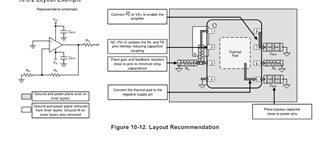
For example in the datasheet of OPA837 it is mentioned as follow:


This raise the following question for me:

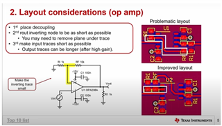
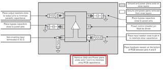
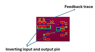
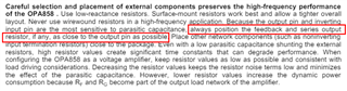
  • Do we need to just remove the GND and PWR plane just underneath the inverting pin and output pin? or also we need to remove the GND and PWR underneath the feedback trace as well?

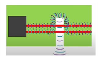
  • My second question would be if we need to remove the GND and PWR plan under the feedback trace as well then we can make another critical problem related to signal integrity. As a general rule for high speed PCBs we need to provide a solid GND plan underneath the signal traces, otherwise it can cause signal integrity issue:

Thanks in advance for your answers and helps:

  • Hi Behnam,

    We have designed PCBs in the past where the planes under the trace were also removed. The OPA855 design, which has performed well for our device GHz device removes the planes under the pin and component pad connected to that pin only. To avoid crossing traces over plane gaps you can follow the same plane design as the OPA855EVM.

    Best Regards,

    Ignacio

  • Hello Ignacio,

    Thank you for your message.

    Would you please share a Altium file of OPA855EVM?

    Regards,

    Behnam,

  • Dear Ignacio,

    In the datasheet of OPA855, they have just remove the GND and PWR under the feedback pin, not for the inverting and out pin, which does not comply with what the datasheet has requested (To reduce unwanted capacitance, cut out the power and ground traces under the signal input and output pins.): 

    Would you please share TI design that has been proven to work correctly?

    Regards,

  • Hi Behnam,

    The datasheet figure has the configuration slightly off. Your best reference would be the OPA855EVM users guide. I also attached the Altium project for that EVM as well.

    Best Regards,

    Ignacio

    OPA85x_Altium.zip

  • Dear Ignacio,

    Thank you very much, you always helped me a lot. I spotted something else to be off, would you please confirm? in the datasheet of OPA855, it is mentioned put the feedback resistor close to the output pin:

    But I expected it should be close to the inverting input pin. I also found another post form TI, which confirms my statement. Please let me know, what do you think? 

    Best regards,

    Behnam,

  • Hi Behnam,

    That was likely taken from a previous datasheet and was not updated. For the OPA855, there is a feedback pin which is used to limit parasitic capacitance. Therefore, the Rf resistor should be as close possible to both the inverting pin and FB pin. The EVM shows the proper way to layout the components around the device.

    Best Regards,

    Ignacio

  • Hello Ignacio,

    Thank you for your thorough explanation. I sincerely appreciate your assistance.

    (Proposal to Enhance Datasheets and Layouts for Amplifiers)

    I would like to extend an offer to Texas Instruments to help improve the quality of their datasheets by implementing best layout practices and update all the datasheets. Additionally, I can provide sample layouts in Altium for all the amplifiers, which could be included in the resources section for each respective amplifier.

    I believe that these enhancements would greatly benefit your customers and contribute to the overall success of their products. I am willing to undertake this initiative as a voluntary activity, or explore other possibilities for integrating my efforts within the company. I am highly motivated to contribute in this capacity.

    I would appreciate your feedback and suggestions on how we can proceed with this proposal.

    Looking forward to your response.

    Best regards,

  • Hello Ignacio,

    Just wanted to kindly follow up on my previous message, Would you please let me know what is your your suggestion? and how we can proceed with this offer? 

    Regards,