This thread has been locked.
If you have a related question, please click the "Ask a related question" button in the top right corner. The newly created question will be automatically linked to this question.
Hello TI,
I've just got some INA333 samples from TI.
I made a circuit to test this, but I have 2 problem.
- Gain always = 2
- Positive signal is cut off.
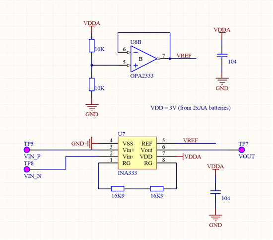
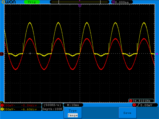
Please take a look at the image below about the circuit and the signal from ossillo.
Channel 1 is signal from function generator( Amp = 500mV, f ~ 35Hz)
Channel 2 is out voltage from INA333. Vref ~ 1.5V
Hai Bien,
Datasheet doesn't mention about the presence of pin 6 and pin 7. Please check the link below
Hi,
Thanks for your reply.
Note that I used OPA2333, dual opamp IC.
I check Vref voltage. It's about 1.5VDC
Bien,
Thank you for your question regarding the INA333. The output signal you are seeing is caused by your input signal being outside the specified input voltage range of the device. The gain you should expect using two 16k resistors is 1+(100k/32k) = 4.125.
I am guessing that your 500mVpp, 35Hz input wave on pin 3 of INA333 has no DC offset and that you have pin 2 set to ground in your test circuit. (Circuit simulation and results shown below). As you can see the simulation's output signal matches closely with your oscilloscope results you have provided.
Many amplifier's (including INA333) operating range (swing) is limited by the positive and negative voltage references (single supply/dual supply, etc) you provide. In your specific application, you have approximately 3V of swing (VDD is two AA batteries). The actual range of the device is listed in the datasheet on the first page under "Input Voltage: (V-) + 0.1V to (V+) -0.1V" and "Output Range: (V-) + 0.05V to V(+) -0.05V." This means that for your application your inputs need to be between 0.1V and 2.9V for the INA333 to operate correctly and your outputs will be limited to a range of 0.05V to 2.95V.
By referencing your inputs to ground (with a single 3V supply), you are already losing "half" of your input signal because the device is not specified to operate correctly when the input signal is less than 0.1V (approximately half of your 500mVpp, 35Hz input signal).
Solution:
One solution to your problem is to reference your (+) and (-) inputs to your "Vref" in a similar way you are referencing your output to "Vref" by using your half supply bias circuit (OPA2333).
See the simulation and outputs below and notice that the input signal and pin 2 on the INA333 are referenced to a common "Vref." This common mode voltage will be rejected by the INA333, and ideally, only the differential voltage between the two input pins will be amplified.
By biasing your inputs to half your supply range (1.5V), this puts the entire input signal within the input range of the device. The device operates correctly and the gain is set to the expected 4.125 V/V which results in the output signal being 500mVpp x 4.125 = 2.1625Vpp. Please let me know if you have any more questions and see the TINA-TI simulation file to change any circuit parameters or to explore more.
As another resource, please check out this video: http://www.youtube.com/watch?v=bg1OwZFtOeM
Hi Michael,
Thank you for the useful guide.
I'm using Funtion Generator to create input signal for INA333. I think it's take the same ground and the signal has no DC offset.
I will change the signal for test INA333 again.
Thank you very much!
You are welcome Bien. I'm glad we were able to help you with your INA333 testing issues.