A related question is a question created from another question. When the related question is created, it will be automatically linked to the original question.
If you have a related question, please click the "Ask a related question" button in the top right corner. The newly created question will be automatically linked to this question.
I wanted to let you know that I finished the analysis and will have an PowerPoint summary of the analysis and recommendations for you by the end of the day.
Thank you very much for your help. I will take a look at your analysis in the next few days. I will probably have some questions to complete my desing.
I read the report and I still have a lot of questions to undersand all the calaculations and the modifications. I would like to be able to do this analysis by my own in the future.
Page 4: Where can I find the information for the tconv graph (why it's 10ns).
Page 5: Where can I find the formulas and the values for the calculations. I found the values for the ADC model in the datasheet but not the other ones.
Qsh formula
Qfh formula (I gest the 0.5 is for 1/2LSB)
Cfh (what is the 100mV)
tsettle (why 0.75)
Tc formula
Toa formula
Fpoa formula
Page 9: Why should we use the MFB configuration. If the Vcm is equal to (v-) to (+V)-1.15V does it means that I would not be able to use the full scale of the ADC (0V to 3V).
Page 9: Where can I find that the noise is x20 at Vcc-1.5V for the OP376.
Page 9: Why should I reduce the resistors value by a decade.
Sorry for the late reply; I was out of office. I have attached 2 presentations that discuss calculation and modeling the ADC and the driver. This research was collaborated over the years between the Op amp and ADC teams. In the future there will be "TI Precision Lab" videos discussing this information. In the mean time I am happy to help and answer any question you have on this material. Below are bullet point answers to the questions you posted in the previous reply.
The pulse in the timing diagram for tconv is to discharge the sampling capacitor before the next sample. Refer to the "SAR ADC Input Drive_2016 RevB " presentation
The calculations and formulas can be found in the "SAR ADC Input Drive_2016 RevB" presentation
MFB topology is a inverting configuration which avoids common mode limitations. This means that you will be able to use the full scale of the ADC (0.1V-3V) with the op amp output limit for linear swing being 100mV from the rails. The Sallen-key topology is a non-inverting configuration where the Vcm is varying with the input signal. This is where you will be limited on full scale based off the Common-mode voltage range of the OPA625 [(V-) to (+V)-1.15V]. Given a supply of +3.3V, the input range as a non-inverting configuration is [0V-2.15V]
The OPA376 is our lowest Vos part without a chopper. For this application it is not recommended because the noise increases when the VCM is within this range [(V+)-1.3V<VCM<(V+)+0.1V]. I have attached a table of the specification within that region that will be included to the OPA376 datasheet in the near future.
In order to have a low offset as the OPA376 as well as low noise, a zero-drift (chopper) amplifier is recommended (OPA378). Because this is a chopper topology, the chopping stage injects some charge directly on the input resulting in input bias current spikes. For this reason, it is recommended having smaller resistance values.
Let me know if you have any more questions on the recommended circuit.
Would it be a good idea to use the same circuit configuration for a 0V to +10V sensor. To use the full scale, I would modify the offset voltage of the first amplifier to 3.0V.
If it's ok to use this confuguration for an unipolar signal, what would be the best way to use the REF5030 to generate the 3.0V offset and the 1.5V offset.
What should be the best design practice for multiple analog inputs. Should I use one buffer for each voltage offset of each channel or use one buffer for multiple channels.
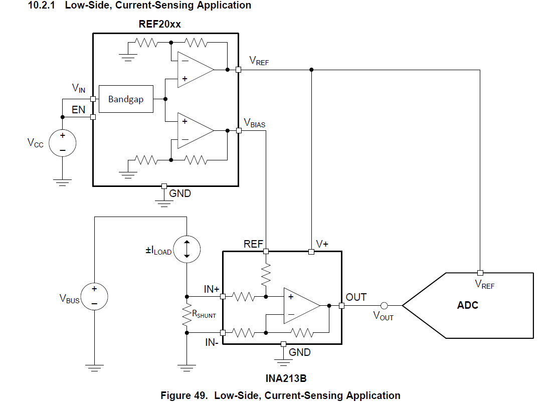
It should be fine to use this configuration as unipolar signal. I would recommend REF2030 this will give you both you an accurate output of 3V and 1.5V without having to deal with resistor tolerances. On page 18 of the REF2030 datasheet, it shows an application example of using Vref for the ADC and Vbias for the offset of a difference amplifier. I have also attached a screen shot of it below.
It would depend on the amount of analog inputs. How many analog inputs? Would the signal chain be the same and the initial design? Would the input be the same as the initial design or are the amplitudes different? Would you be able to draw a quick sketch so I can make sure we are on the same page.
After reviewing the pdf I would recommend that you tie the Vref and Vref/2 channels directly to the REF2030. The REF2030 is able to supply up to 20mA of current. From analyzing all the channels in your pdf with the REF2030, it should be able to drive all the channels. One of the key features of the REF2030 outputs tracks each other with a precision of 6ppm/C across the temperature range of -40C to 85C. The op-amps used for buffering VREF and VREF/2 will not only add to the overall system cost, but will affect the precision of REF2030 due to the offset and drift that the op amp contributes.
We tried to test the ADC with the same circuit configuration you suggested us and the REF2030 for the voltage reference. When we measured the Vbias (Vref/2) with the ADC the signal seems very noisy. The output values are around 2048 with a noise of +/-35 counts. We also tried different voltage sources with the same results.
I read the following application report and the recommended value for Cfilt is more higher than the value you recommended (220pF vs 115nF). We tried different values of Cfilt and Rfilt to reduce the noise. With a capacitor of 1uF and a resistor of 20Ohm we have better results but it still noisy. The ouput values for Vbias are around 2048 with a noise of +/-10 counts.
Do you have any recommadation to get better results? What is the source of this noise?
We found one problem but still have stange behavior with the ADC. The first problem came from the voltage follower buffer connected to the REF2030.
The output of each voltage follower was very noisy. Do you know why the OPA378 was so noisy at the output. Is this came from the voltage follower configuration.
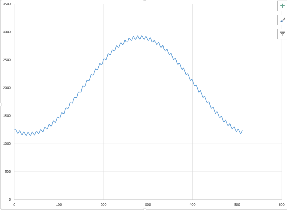
Now we face a problem with the ADC sampling. For some reason we often see multiple samples with the same value. For example, if we have a 60Hz 1Vpp sine wave at the input, we measure a signal of 63.5Vpp at the ouput of the voltage divider. The following image shows the result of the conversion.
Do you have any idea why we get this kind of result.
Looking at the schematic, the capacitance load is too large and is cause instability in the circuit especially with a zero-drift device. The REF2030 device is designed to be able to handle the capacitance max of 10uF for the load. I will post a PowerPoint later today showing simulations and recommendation on the schematic posted.