This thread has been locked.
If you have a related question, please click the "Ask a related question" button in the top right corner. The newly created question will be automatically linked to this question.
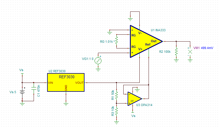
Hi, I want to your help to design reference drive circuit for the ina333. The INA333 in my circuit is powered from ref3030 i.e 3V and i want to give 500 mV to the REF pin of the ina333. The most commonly use opa333 is very very costly for our product budget. Can you suggest a cost effective solution for this?
The driver circuitry cost can be more around 0.1 to 0.2 USD.
Thanks in advance!
Vidula,
Since you use a lower precision, 0.2% initial accuracy reference voltage, REF3030, there is no point on using high precision, more costly op amp for driving REF pin of INA333. Therefore, the cost effective solution would involve using OPA314 or OPA313 as shown below.
You could also consider using INA326 for your solution, which unlike INA333 would give you rail-to-rail input common-mode voltage range.INA333 Vidula circuit.TSC
Thanks for your suggestion. I will check with opa314 and opa313. INA326 is costlier than ina333 so we might not use that.
Query:
1) We are using ina333 for load cell output amplification.Load cell is powered from same ref3030 so at input of the ina333 the voltage is Vin+= 1.489 V and Vin= 1.489 V. Is it a proper setting or i need to change something. if you want to refer schematic then please let me know i will send you in private i cant share it on forum.
Vidula,
The circuit should work just fine and for the input common-mode voltage of 1.489V should result in the maximum output voltage range of 50mV<Vout<2.95V - see below. I have assumed below a gain of 100 but if your gain is different, the maximum input differential voltage, (Vin+)-(Vin-), will have to be adjusted to reflect the actual gain.