This thread has been locked.

If you have a related question, please click the "Ask a related question" button in the top right corner. The newly created question will be automatically linked to this question.

INA240: Output linearity

Guru 54428 points
Part Number: INA240
Other Parts Discussed in Thread: EK-TM4C1294XL, TMS320F280049C, TMCS1101

Hello,

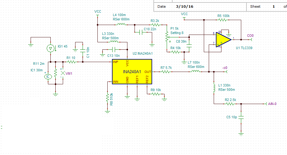
Recently did new experiment with small Nidec 12 pole motor and three 240A1's, REF1/2 mid supply (1.65v), VS=3.34v. Contrast REF1/2=GND all three 240's on a separate sub PCB sit just above shunt in both experiments. The three sub PCB grounds separated individual wire feed into the target MCU ground plane isolated from shunt ground. 

The ADC conversion values per millivolt for the same amount of current load in each experiment differed greatly. The 1.65v mid supply flat lined at 1.6 amps increased maybe 100mA upon adding any amount off additional current load. Yet the experiment where REF1/2=GND the output rose 1.6A and upon adding current load the ADC samples easily traverse past 2.1 amps. In each experiment the single ended ADC channels and conversion scale factor 0-4096 was configured to show steady state near 1.6A. 

The main difference being first experiment ADC incremented from 0.1,.2,.3.4,.5,.6,.7,.8,.9 etc. up to 1.6A and the second (REF=mid supply) jumped to 1.6A skipping over all lower values. The ADC conversion calibration was derived from the Nidec motors run time steady state load current in both experiments. What happened to the open loop linearity in the second experiment?

There seems to be an issue that output open loop linearity divides in half for REF set mid supply (1.65v) thus affecting ADC granularity near scale 2048. How can this be occurring in the ADC when the full scale is 4096 in each experiment? Is there some kind of counter measure inside some TI ADC modules expecting a division in open loop output linearity analog signals fixed to a 1.65v threshold? Perhaps analog converters require band gap (1.65v) to maintain bidirectional REF open loop output linearity? Seemingly that is not required in unidirectional REF configurations such that INA output maintains full scale (4096) open loop linearity.


  • What is best undocumented way to make INA produce bidirectional output from ground side position just like traditional discrete amplifiers do. How has the 240 not lived up to datasheet claim it can replace discrete high bandwidth amplifiers that easily measure bidirectional current from 0v up to nearly supply rail?

    Has it occurred both shunt zero crossing cycles do exist on the same output polarity of high bandwidth discreet amplifiers? This how it was working in the past but not with bidirectional INA which divides zero crossing events to do that. For example AC in circuits there is no such thing as negative watts as they cancel out into positive values derived from positive measured current events.

    It would seem reasonable to believe any DC inverter, watts are derived via mostly positive current (P=EI) adding/subtracting (min/max) perturbations or AC electrical theory is making this up?      

  • Hi,

    It would be helpful if you could provide a schematic and tabulated measurement results.

    However you stated “The three sub PCB grounds separated individual wire feed into the target MCU ground plane isolated from shunt ground”. Please note that the shunt ground shouldn’t be isolated from the INA240 ground. This can cause potentially large distortion.

    Regards, Guang

  • Hi Guang,

    Guang Zhou said:
    It would be helpful if you could provide a schematic and tabulated measurement results.

    Verbatim I explained the current measure behavior both experiments, please read the text in both experiments. Schematic for known REF modes seems your reaching rather than investigate the issue. Single PCB with ground plane on back side, one INA240 each PCB and accurate bidirectional current monitor is not possible with this INA device from ground side.


    Guang Zhou said:
    However you stated

    Umm that would then imply pin 1 & 4 should be connected to pin 3 kelvin connection but are actually isolated common grounds not on the same wire path. Experiment has a TI launch pad EK-TM4C1294XL and 3 phase DC inverter 3 sub PCB only touch pin 1,2 of shunt kelvin connection sitting to one side of shunts. Our custom PCB with same MCU has the exact same problem as pin 1,4 same ground of pin 3. Then we see the TMS320F280049c the 12 bit SAR ADC converter has 1.65v band gap and full 3v3 reference that our ADC does not have band gap.

    Please answer why discrete amplifier in same low side position work with Launchpad ADC to produce correct bidirectional current results from full scale 0v-3v3?  Yet INA fails profusely to produce full linear results in this mid supply REF from low side? My thought is TI has not fully understood the past method of discrete high band width amplifier in low side monitoring and made vague datasheet statements that it can. But we discover only in unidirectional current measure being realistic. And far from being factual relative to single discrete amplifier behavior in the same low side position! 

    This schematic produces fairly accurate bidirectional current measures from discrete amplifiers but same 3 INA can not!

     Past to show forum Tina model of INA with inverting pin 3 has 510k resistor and produce almost same wave form as discrete HBW amplifier but REF=GND is not exactly correct. Can FE try further Tina testing to determine how to maintain precision from relative same bidirectional configuration has better precision than my model?


  • Hi,

    To avoid ambiguity, we need to look at your schematic and a picture of the PCB setup.

    Regards, Guang

  • Again unidirectional works mostly as datasheet claims and low side bidirectional produce locked scale ADC results +/-75mV relative to mid supply (1.65v), no further current load detection occurs. Yet bidirectional scope gain increases magnitude but no detectable or greater ADC count occurs +/-0.075v in custom or experiment PCB's. The custom PCB even has dedicated 3v3 LDO regulator for INA devices producing +5v switch isolation. The experiment 3x INA240 used launch pad 3v3 LDO. This is not an issue with layout or INA configuration rather an issue of device compatibility.

    Perhaps you can point out (Wiki) how bidirectional current measure theory produces magnitude in the ADC counts? Seemingly as current increases so should the ADC converter digital count grow, well above 2048 up to full scale 4096. Yet in my mind the split full scale 0-2048 and 2048-4096 makes no sense being the crossing counts tend to cancel each other out near midRef +/-0.075v as is occurring! And as the bidirectional current load increases the worse this issue is.

    That seems to be the case why the ADC refuses to produce count values much above or below 1.65v being mid REF 1.65v +/-75mv. It seems this TI ADC needs internal counter measures for mid supply crossing events AKA band gap (1.65v) circuit not all TI ADC seem to have. What occurs now is the internal charge share capacitor saturates inside the ADC as it does can not produce scale changes much above or below 2048 counts.

    Seemingly there is an SAR compatibility issue the datasheet does not confront. The datasheet claim to replace discrete amplifiers is perhaps misplaced as the INA240 can not achieve low side bidirectional full scale measure in this ADC from mid supply REF. Has TI forum FE attempted to confirm as we have using the EK-TM4C1294XL launch pad and the INA240 EVM this is even possible?


  • Guang Zhou said:
    To avoid ambiguity, we need to look at your schematic and a picture of the PCB setup

    This is an experiment based from datasheet stated facts that fail to produces proper results via TI own test beds. Guang please have some respect for this TI guru and do your own testing with the TI tools readily available. Otherwise this is a waste of our time too and no one wins.

    I can PM you pictures simple schematic but that is not going to end debate of INA configuration and ADC compatibility issue.  

  • Hi,

    Please post your schematic and relevant documentation here. It is the most efficient way of communication.

    Only then can we discuss next course of action.

    Regards, Guang

  • Hi Guang,

    /cfs-file/__key/communityserver-discussions-components-files/14/INA240x3-Experimental-Schematic.pdf

    For this PWM modulation one phase is always OFF any two being ON of three. Meaning one INA forces ADC input center (1.65v) 2048 every current cycle as the other two INA are being restricted +/- 75mV around 2048 count. So the 2 counts never increase relative 1.65v threshold but does not affect lower value samples on the other non INA inputs. There are also millisecond gaps all 3 signals where the output has steady state 1.65v, blank air time. INA unidirectional signal does not produce that restricting artifact into the ADC.

     The discrete amplifier shown above produces zero crossing artifacts without saturation of mid point ADC 2048. Again the discrete amplifier inverting input is not clamped to ground so negative cycles invert into a fully positive signal pulse train originating from 0v. Thus removing fixed center artifacts from the signals where there is NO interval blanking possible on the ADC converter. That means a bidirectional centered signal is not fully compatible with the ADC if the output remains on during dead air time.

  • Hi,

    I don’t completely understand what you mean by “restricting artifact” and the discrepancies between your two configurations in general.

    Can you post pictures of your setup, together with oscilloscope captures of the INA240 output (before the 5.7K resistors)?

    Regards, Guang

  • Guang Zhou said:
    I don’t completely understand what you mean by “restricting artifact” and the discrepancies between your two configurations in general.

    The restricting artifact is the mid supply REF (bidirectional) current measure saturates at the ADC level. Yet ground REF (unidirectional) does not!

    Guang Zhou said:
    Can you post pictures of your setup, together with oscilloscope captures of the INA240 output (before the 5.7K resistors)?

    Where are any TI scope captures of INA or SAR ADC output proving datasheet claim is indeed factual to begin with?

    The single ended ADC channel seems to experience bipolar current reversals and some how cancel out sampling magnitude +/-75mV of mid supply (1.65v). Yet INA unidirectional via same circuit has no such issue but does not produce proper generator current analog signal as does the TI discrete amplifier circuit shown above post. Scope captures are meaningless to post, will not prove bidirectional INA amplifier is ever compatible with this SAR ADC. 

    We need INA properly configured bidirectional where inverting input (-IN) has not bean directly tied Kelvin ground. Bidirectional INA  saturates ADC sample hold window well below the actual load current. Nidec 1.6 amp motor load proves the INA bidirectional configuration of schematic and datasheet is not viable for all SAR ADC via low side placement. The bidirectional INA is not producing a proper output the SAR or software can compensate these incompatible current reversals crossing mid supply 1.65v.

    The unidirectional INA produces Nidec motor unloaded current 1.6 amps, loaded >2.5 amps.  Please explain how that is possible but not via bidirectional? 

    Perhaps bidirectional configuration behaves differently with SAR when INA is place inline than it does from low side monitor positions?

    It would seem bidirectional INA output analog current reversals directly inflict SAR in a bad way from 3 low side monitor positions! How has this posted issue escaped the attention of INA silicon designers? 

  • Hi,

    The datasheet gives a detailed description of common configurations in section 8.4.2, including the ones you mentioned. Please refer to it.

    You said ADC is saturated in bidirectional configuration and not in unidirectional. Please provide scope shots of INA output so that we can decide if it is due to INA output being saturated. This is a necessary step in isolating the problem.

    Regards, Guang

  • Guang Zhou said:
    Please provide scope shots of INA output so that we can decide if it is due to INA output being saturated.

    It was thought to be sequencer step saturation and recently discovered unidirectional analog signal is phase shifted shifting. Analog signal is missing from where it should be occurring in the triggered acquisition window. So unidirectional sampled very late in PWM commutation can produce deceleration linear slope versus serpentine current pattern. Yet late triggering samples has much greater low end error % relative to INA shunt calculator results and other external test equipment.

    The INA shunt calculator error values are from SAR acquisitions in either REF current mode. And or after arbitrary ADC calibration required to compensate for phase shifted analog signal occurring in the wrong PWM window frame time. Triggering ADC is an industry calculated event typically occurs via center load count of 1st generator. Somehow INA signal is shifted to 3rd generator comparator B down and produces excellent linear slope attributes but low end error % is greater. So steady state external 100A bar on low side digital show 4.5 amps and INA thinks >8.2 amps to ADC. And 8.2A via 100A bar is close to INA samples but peaks no further >8.7A when 100A bar may show 9.2A - 10A peaks during motor acceleration. Discrete amplifier does not phase shift the PWM triggered acquisition window or omit negative 1/2 cycles and remains synchronous with PWM generator 1 center count load times.   

    How can it be shown via scope captures INA is phase shifting output and missing the inverted analog signal required for SAR window? So far only 240us ADC triggering and settling produce close to INA shunt calculator results, versus 20us samples via comparator B down triggers. These INA results are not very encouraging or at all professional! 

    https://e2e.ti.com/support/microcontrollers/other/f/908/p/870294/3230196#3230196

  • Hi,

    It helps to break down the problem into manageable parts. I assume you have to know the right vs wrong INA240 output.

    If you continue to suspect INA240 is the source of the problem, please present evidence, including schematic, test setup, scope shots and reasoning behind your argument.

    Regards, Guang

  • Guang Zhou said:
    If you continue to suspect INA240 is the source of the problem, please present evidence, including schematic, test setup, scope shots and reasoning behind your argument.

    Schematics are present above post. Scope captures unidirectional has voids discrete amps above schematic do not produce where the ADC can sample very low phase shifted values via Comp B down ADC triggers. The actual shunt error resulting due to these voids is 10x the INA shut calculator predictions, especially in low end samples. Initial output gain from odd PWM signals during open loop commutation distort samples results.


  • Unidirectional INA barely works to measure low side motor load current greater than a few amps and is plagued with precision error well beyond the INA shunt calculator predictions. The discrete amplifier had similar issues via low side 18mohm shunt during motor open loop. Yet the discrete amplifier remained extremely linear in closed loop commutation producing 0 data voids or loss of measured amps as does the INA240 even from 240µs sample intervals. 

    The precision error from a 2mohm Vishay metal shunt is at lest 10x greater than INA shunt calculator predictions on low end >0.5mA. I really can not justify how a 3mohm shunt will reduce this amount of precision losses. Unless the INA circuit is greatly modified to include zero crossing shunt data on the inverting input to act much like discrete amplifiers great linearity without any PWM rejection at all. Otherwise the INA as datasheet has depicted use with SAR ADC is complete nonsense!

    /cfs-file/__key/communityserver-discussions-components-files/14/1780.Total_5F00_Error_5F00_vs_5F00_Sensed_5F00_Current_2D00_-0.5A_2D00_50A-2mOhm.csv

  • Point being the unidirectional analog signal TI adopted INA series is not fully compatible with SAR ADC >50ns of phase jitter on the output. The mid supply REF suffers the same ADC issue since the same jitter miss aligns 50µs PWM period triggered samples with void data. The industry standard trigger ADC center  PWM periods (load count) produces almost no linear slope as current rises and falls in either mode. 

    It is only by chance I recently decided to test comparator B down via last PWM generator order to produce synchronous ADC triggers relative to INA phase jitter. Was typically aware 200µs phase jitter existed but never dreamed it could result in asynchronous serpentine samples motor deceleration. Jitter also seemed to stop linear slope from being developed without 240µs blanking intervals triggering ADC samples. That timer blanking method shifted the SAR acquisition window much like comparator B down via last generator and compensated for the INA output phase jitter, only to some degree not entirely!

    This same INA output shifting jitter occurs no matter how or where INA has been mounted low side. Added series resistance or capacitance values around the VS pin have absolutely no affect to reduce phase jitter. Hence the INA output must produce a contiguous analog signal with no 0 volt voids in either direction as the above modified -IN scope capture. A seamless analog signal of both zero crossing events is produced as discrete amplifiers of the past would.

  • The above capture derived from Nidec motor steady state current 1.6 amps. Why on earth is 240 output phase shifting >200µs when the PWM CH1 falling edge only reduced shunt falling edges by only 50µs. The PWM CH1 rising edge does not ever change yet CH2 the entire signal shifts (bops) to the left >200µs most often.

    The ADC is triggered via PWM (CH1) and the actual peak cycle amps are almost never being sampled since CH2 signal is often absent last few 50µs PWM cycles (right side). That is why the INA shunt calculator error results are 10x greater than predicted on the low end. Thus the low end CH2 output is shifted left into the first few PWM 50µs cycles (CH1) thereby increasing the actual measured current by the same slope amount in open loop commutation.

    CH2 shifting in both directions relative to fixed CH1 worsens at lower motor speeds and becoming asynchronous to ADC sample periods. Scope hold off and pulse trigger width has no effect to stop CH2 signal from bouncing side to side of CH1 50µs cycle periods. Some how the entire INA output signal CH2 shifts (left/right) mostly from the center of CH1 loosing the fixed and synchronous ADC sample window in the process. Yet at low motor current the ADC manages to keep a fairly consistent steady state measure going via RMS calculations.

    All in all the accuracy of low side current ADC measures are severely impacted via output phase shifting shown in CH2 first capture. Seemingly phase shifting is due to INA 300KHz low bandwidth where 3Mhz would not likely shift output to this same degree. The same question remains relative to mounting the INA low side versus in line some how causing severe issues needs to be investigated by TI engineers and not the customer falling victim.  

  • Motor graph never predict FOC open loop startup current >4.5 amps. Yet that often results of the 2mohm shunt and ADC scale factor after software calibration steady states near 1.6amps @5300 RPM, being conservative. We drive the 3 phases with our DC inverters PWM and 24 volt DC supply.

    That same ADC calibration can not be used for large motor >5 amps since it then can not sample 10 amp peak, no load. Obviously bigger motor ADC calibration bumps up open loop current samples. Very odd since DC power supply calibrated 100 amp bar digital readout starts 0.1-0.2 amps (150vdc) as  ADC scope widget show 3-5 amps motor accelerate to closed loop near 86 RPM.  

  • Hi,

    Looks like you started anther thread, I’ll close this one and focus on the new one instead.

    Regards, Guang

  • Please refer to this post as reference since this issue is not so easy to detect and my be due to the low side placement versus inline!  We need some other TI monitor device with the same pin orientation to replace the INA-240.

    Oddly the TMCS1101 with 1.8mohm embedded shunt was not produced with the INA elongated TSSOP8A footprint.   Case size makes it difficult to test via our several custom PCB layout. But HALL isolation should produce more accurate results than INA240 in same low side position?