This thread has been locked.

If you have a related question, please click the "Ask a related question" button in the top right corner. The newly created question will be automatically linked to this question.

LMK03000: PLL lock is unstable with N divider output is slightly high

Part Number: LMK03000

Hi,

The EVM works fine with the attached file settings, but the customer's board has an unstable PLL lock and outputs a slightly higher frequency (all 5 prototype PCBs are the same).

LMK03000設定キャプチャ.xlsx

I monitored the R and N divider / 2 outputs from the MUX to investigate the cause.
The R divider / 2 output was normal, but the N divider / 2 has a slightly higher frequency (since N-div = 3.84MHz, the MUX out was originally 1.92MHz, but it was a 2.08MHz output).

I thought that the input level to the VCO was low and asked to raise the CP current by register setting, but it was already Max, so I could not solve it.

The power supply is an external regulated power supply (the same power supply as for EVM).

What's wrong? Do you have any advice for improvement?
The R divider is normal, so at least I think the REF IN is good.
Is it a problem with the PCB layout?

Best regards,

Hiroshi

  • Hello Hiroshi,

    if the N divider output is slightly higher then expected, the VCO is running at a higher frequency. Thus the device is not locked.

    This can have multiple causes:

    1. OSCin_FREQ register not set correctly and therefore VCO calibration wrong. - please check

    2. too noisy input - please check

    3. loop filter / CP setting not optimal - settings seem to be ok.

    4. schematic/layout issues - please share

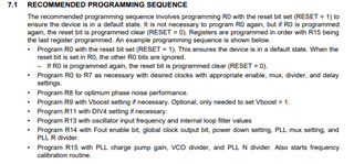
    5. incorrect programming sequence. - please check

    regards,

    Julian

  • Hi, Julian-san,

    I confirmed with the customer.
    1  I tried both "OSCin_FREQ = 3MHz, 4MHz" for input frequency = 3.84MHz, but the status did not change.
    2  I investigated the external signal generator and power supply, but there seems to be no problem. These are the same as for EVM.
    4  I got the circuit diagram and PCB layout.

    回路図.pdf

    基板図.pdf

    The TOP layer is P6 and the BOTTOM layer is P11.

    5  I removed the writing line from the FPGA and wrote from USB ANY2, but there was no change.

    I'm checking this material, but I just wanted to inform you about customer response.

    Best regards,

    Hiroshi

  • Hiroshi-san,

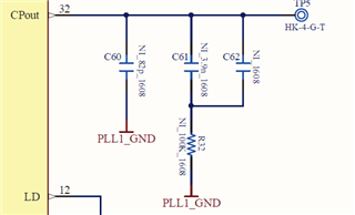
    I see that the components on pin 32 (CPOUT) are marked with "NI". Does this mean that those are not assembled?

    These components are critical to ensure a stable loop. 

    Regards,

    Julian

  • Hi Julian-san,

    I've confirmed.

    C60(C1) 0.15nF,  C61(C2) 8.2nF,  R32(R2) 2.2kΩ

    C62 was not implemented.

    Is there a problem with this Loop filter?

    To check the VCO output, I turned on EN_Fout and monitored Fout, but it remained at GND level. Will it not output unless the PLL is locked?

    Regards,

    Hiroshi

  • Hiroshi-san,

    did you try to do ABA swaps of the units? Customer PCB unit to working EVM and EVM unit to customer PCB?

    When you say "it works on the EVM" do you also have the loop filter values as on customer board?

    I also don't see the AC coupling for the OSCin port on the customer schematic. Can you confirm that this is implemented?

    regards,

    Julian

  • Julian-san,

    Thank you for your support.
    I asked the customer to investigate the difference between a past board that worked fine and a new board that didn't work.

    I make this thread "solved".