This thread has been locked.

If you have a related question, please click the "Ask a related question" button in the top right corner. The newly created question will be automatically linked to this question.

LMK05318B: Cannot DPLL lock - PPS and 24 MHz input, 40 MHz clock output

Part Number: LMK05318B
Other Parts Discussed in Thread: USB2ANY, , LMK05318, LMK5B33216

Tool/software:

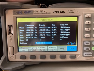
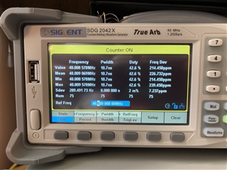
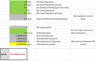
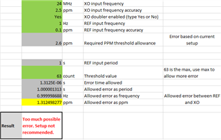
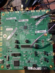
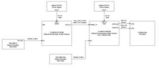
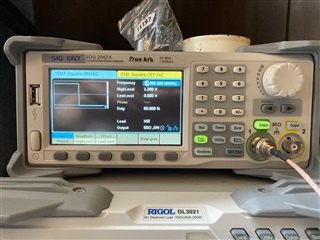
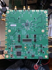
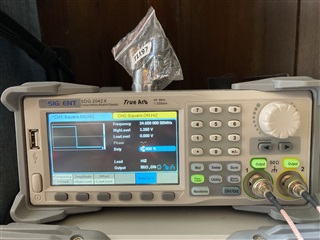
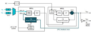
We have implemented the LMK05318B for use in a digital carrier board, to provide a reference 40 MHz set of signals to an RFIC and FPGA. We use a 24 MHz XO that has a +/- 2.5ppm accuracy and a GPS receiver from u-Blox to provide a PPS input.

I'm attaching our TCS file: https://drive.google.com/file/d/1yKAOyZ3CsoECdfFrOq-e86CL_EgNNyhQ/view?usp=drive_link

And the carrier board's schematic page: https://drive.google.com/file/d/1t9dCRsU3_SJ7NDb1n1_-0KC1_oprw6b2/view?usp=sharing

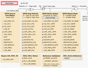
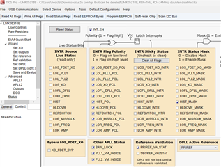
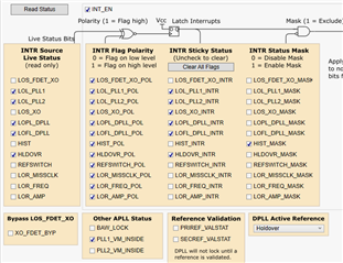
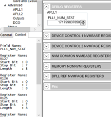
We have the following status bits when we flash our LMK chip:

  • 'LOL_PLL1': 1
  • 'LOL_PLL2': 1
  • 'LOS_FDET_XO': 0
  • LOS_XO': 0
  • 'HIST': 0
  • 'HLDOVR': 1
  • 'LOFL_DPLL': 1
  • 'LOPL_DPLL': 1
  • 'LOR_AMP': 0
  • 'LOR_FREQ': 0
  • 'LOR_MISSCLK': 0
  • 'REFSWITCH': 0

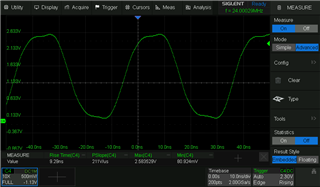
Meaning that our LMK chip's DPLL cannot lock on, even after waiting for several hours (~12 hours) to the lock to be established. We have measured the pps signal and XO input and they are valid signals, using an oscilloscope. The LDO power supplies are working properly.

Any input and recommendations to achieve a DPLL lock would be appreciated, or further debugging steps.

  • Hi Arpad,

    Can you please upload the .tcs and schematic to the e2e forum? I am unable to open the Google Drive. If you click Insert then Image/video/file, you should be able to upload.

    I'm also observing that APLL1 is not locked (LOL_PLL1). If the APLL does not lock, then the DPLL will not lock. There is either a configuration issue or setup issue. Let me take a look at the .tcs file once you upload it to e2e.

    Regards,

    Jennifer

  • Hi Arpad,

    1. I did not see the schematic PDF get attached to the last post. Can you please share it through e2e?
    2. How are you programming the LMK05318B? Through the external USB2ANY dongle? This is a test on your custom carrier board not the LMK05318BEVM, correct?
    3. Please try with the attached .tcs file. I widened the LOPL thresholds and lowered the BAW_LOCK thresholds. This won't impact the APLL1 lock but the registers are now configured to recommended settings.
      1. 2025-04-11, ti-2.tcs
    4. Also, try clicking on the Soft Reset Chip button in the toolbar to toggle the SWRST register. This issues a PLL recalibration and should be triggered when APLL settings are modified after start-up. Then, resend a picture of the Status Page, making sure to click on the "Read Status" button first.
    5. Lastly, can you please send scope shots of the PRIREF 1PPS input and the OUT7 1PPS output?

    Regards,

    Jennifer

  • DigitalCarrierBoard_LMK_Schematics.pdf

    Hi Jennifer,

    Thank you for the feedback. I've provided the schematic page above.

    The custom carrier board is programmed using a python script that programs the LMK05318 via I2C. We use the EEPROM instructions file, flash it to the device, and then reset the LMK chip as recommended in the datasheet procedure to program it.

    We will attempt the programming procedure with the updated .tcs file.

    We have attempted issuing a Soft Reset command to the chip (via I2C) to re-calibrate but that does not change the result. We will try that step again with the updated .tcs file.

    Yes, we can collect scope probe results.

  • Hi Arpad,

    Thank you for providing the schematic PDF. I reviewed and do not see concerns.

    Please also perform these additional steps:

    1. Probe each VDD and VDDO pin to make sure power is delivered to the pin as expected.
    2. Perform a readback of the registers programmed and compare with the file used to program. We need to confirm that the EEPROM programming was successful and the registers are getting programmed as you would expect.
    3. Readback the BAW_LOCK register, R80[7]. This register captures the state of lock between the XO input frequency and the VCO1 output frequency.
    4. Readback PRRIEFVALSTAT, R411[2] and SECREFVALSTAT, R411[3]. This register captures the state of validation for the DPLL references.
    5. Take a scope shot of the the XO input, as closest to the pin as you can probe.

    Regards,

    Jennifer

  • Hi Jennifer,

    We are testing your .tcs file on the LMK05318B EVM and have some data, as well as questions. Video below shows TICS Pro + Scope.

    R0	0x000010
    R1	0x00010B
    R2	0x000235
    R3	0x000342
    R4	0x000419
    R5	0x000511
    R6	0x000618
    R7	0x000703
    R8	0x000802
    R10	0x000ACA
    R11	0x000B0F
    R12	0x000C1B
    R13	0x000D00
    R14	0x000EC0
    R15	0x000F00
    R16	0x001000
    R17	0x00111D
    R18	0x0012FF
    R19	0x00130D
    R20	0x0014F8
    R21	0x001501
    R22	0x001600
    R23	0x001755
    R24	0x001855
    R25	0x001900
    R26	0x001A00
    R27	0x001B00
    R28	0x001C01
    R29	0x001D13
    R30	0x001E40
    R32	0x002044
    R35	0x002300
    R36	0x002403
    R37	0x002500
    R38	0x002600
    R39	0x002702
    R40	0x002803
    R41	0x002900
    R42	0x002A11
    R43	0x002BC2
    R44	0x002C00
    R45	0x002D03
    R46	0x002E88
    R47	0x002F07
    R48	0x003040
    R49	0x003141
    R50	0x003217
    R51	0x003300
    R52	0x003400
    R53	0x003513
    R54	0x003600
    R55	0x003700
    R56	0x00380F
    R57	0x003900
    R58	0x003A0F
    R59	0x003BBF
    R60	0x003C2F
    R61	0x003D00
    R62	0x003E63
    R63	0x003F3C
    R64	0x004095
    R65	0x004102
    R66	0x0042F8
    R67	0x0043FF
    R68	0x004408
    R69	0x004500
    R70	0x004600
    R71	0x004700
    R72	0x004828
    R73	0x004900
    R74	0x004A00
    R75	0x004B00
    R76	0x004C00
    R77	0x004D0F
    R78	0x004E00
    R79	0x004F11
    R80	0x005000
    R81	0x00510A
    R82	0x005200
    R83	0x00530E
    R84	0x005410
    R85	0x005500
    R86	0x005600
    R87	0x00571E
    R88	0x005884
    R89	0x005980
    R90	0x005A00
    R91	0x005B14
    R92	0x005C00
    R93	0x005D0E
    R94	0x005E10
    R95	0x005F00
    R96	0x006000
    R97	0x00611E
    R98	0x006284
    R99	0x006380
    R100	0x006428
    R101	0x006501
    R102	0x006622
    R103	0x00670F
    R104	0x00681F
    R105	0x006905
    R106	0x006A00
    R107	0x006B64
    R108	0x006C00
    R109	0x006D34
    R110	0x006E15
    R111	0x006F55
    R112	0x007055
    R113	0x007155
    R114	0x007255
    R115	0x007303
    R116	0x007401
    R117	0x007500
    R118	0x007600
    R119	0x007700
    R120	0x007800
    R121	0x007900
    R122	0x007A00
    R123	0x007B00
    R124	0x007C00
    R125	0x007D00
    R126	0x007E00
    R127	0x007F00
    R128	0x008001
    R129	0x008101
    R130	0x008200
    R131	0x008301
    R132	0x008401
    R133	0x008577
    R134	0x008600
    R135	0x008729
    R136	0x008800
    R137	0x008917
    R138	0x008A0C
    R139	0x008B03
    R140	0x008C02
    R141	0x008D00
    R142	0x008E01
    R143	0x008F01
    R144	0x009077
    R145	0x009101
    R146	0x009289
    R147	0x009320
    R149	0x00950D
    R150	0x009600
    R151	0x009701
    R152	0x00980D
    R153	0x009929
    R154	0x009A24
    R155	0x009B00
    R156	0x009C16
    R157	0x009D00
    R158	0x009E00
    R159	0x009F00
    R160	0x00A0FC
    R161	0x00A100
    R162	0x00A2C8
    R164	0x00A400
    R165	0x00A500
    R167	0x00A701
    R178	0x00B200
    R180	0x00B400
    R181	0x00B500
    R182	0x00B600
    R183	0x00B700
    R184	0x00B800
    R185	0x00B9F5
    R186	0x00BA01
    R187	0x00BB00
    R188	0x00BC00
    R189	0x00BD00
    R190	0x00BE00
    R191	0x00BF00
    R192	0x00C050
    R193	0x00C118
    R194	0x00C218
    R195	0x00C33F
    R196	0x00C4FF
    R197	0x00C5FF
    R198	0x00C63F
    R199	0x00C7FF
    R200	0x00C8FF
    R201	0x00C900
    R202	0x00CA3F
    R203	0x00CBFF
    R204	0x00CCFF
    R205	0x00CD3F
    R206	0x00CEFF
    R207	0x00CFFF
    R208	0x00D000
    R209	0x00D114
    R210	0x00D200
    R211	0x00D316
    R212	0x00D400
    R213	0x00D514
    R214	0x00D600
    R215	0x00D716
    R216	0x00D800
    R217	0x00D900
    R218	0x00DA00
    R219	0x00DB00
    R220	0x00DC01
    R221	0x00DD03
    R222	0x00DE93
    R223	0x00DF87
    R224	0x00E000
    R225	0x00E100
    R226	0x00E200
    R227	0x00E300
    R228	0x00E401
    R229	0x00E503
    R230	0x00E693
    R231	0x00E787
    R232	0x00E800
    R233	0x00E910
    R234	0x00EA10
    R235	0x00EB02
    R236	0x00ECDC
    R237	0x00ED6C
    R238	0x00EE00
    R239	0x00EF02
    R240	0x00F0DC
    R241	0x00F16C
    R242	0x00F200
    R243	0x00F33F
    R244	0x00F43F
    R249	0x00F921
    R250	0x00FA00
    R251	0x00FB03
    R252	0x00FC6D
    R253	0x00FD00
    R254	0x00FE00
    R255	0x00FF00
    R256	0x010000
    R257	0x010101
    R258	0x010200
    R259	0x010301
    R260	0x010402
    R261	0x010580
    R262	0x010601
    R263	0x01072A
    R264	0x010805
    R265	0x0109F2
    R266	0x010A00
    R267	0x010BA0
    R268	0x010C04
    R269	0x010D00
    R270	0x010E02
    R271	0x010FC2
    R272	0x011000
    R273	0x011100
    R274	0x011200
    R275	0x011316
    R276	0x011416
    R277	0x011516
    R278	0x011600
    R279	0x011700
    R280	0x011800
    R281	0x011900
    R282	0x011A00
    R283	0x011B00
    R284	0x011C1E
    R285	0x011D1E
    R286	0x011E00
    R287	0x011F00
    R288	0x012000
    R289	0x012100
    R290	0x012203
    R291	0x012322
    R292	0x012409
    R293	0x012501
    R294	0x012600
    R295	0x01272C
    R296	0x01280A
    R297	0x01290A
    R298	0x012A0A
    R299	0x012B01
    R300	0x012C00
    R301	0x012D1C
    R302	0x012E1E
    R303	0x012F01
    R304	0x01300F
    R305	0x013104
    R306	0x013261
    R307	0x0133F8
    R308	0x013443
    R309	0x0135C3
    R310	0x0136C3
    R311	0x0137C3
    R312	0x0138C3
    R313	0x0139C3
    R314	0x013AFF
    R315	0x013BFF
    R316	0x013CFF
    R317	0x013DFF
    R318	0x013EFF
    R319	0x013F03
    R320	0x014000
    R321	0x01410A
    R322	0x014200
    R323	0x014300
    R324	0x014400
    R325	0x014501
    R326	0x014606
    R327	0x014735
    R328	0x014875
    R329	0x01490B
    R330	0x014A00
    R331	0x014B64
    R332	0x014C00
    R333	0x014D00
    R334	0x014E30
    R335	0x014FD4
    R336	0x015006
    R337	0x015135
    R338	0x015275
    R339	0x01530B
    R340	0x015400
    R341	0x015500
    R342	0x015600
    R343	0x015700
    R344	0x015800
    R345	0x015900
    R346	0x015A02
    R347	0x015B00
    R348	0x015C00
    R349	0x015D00
    R350	0x015E00
    R351	0x015F00
    R352	0x016000
    R357	0x016528
    R367	0x016F28
    R411	0x019B04
    

    Screenshots:

    Scope inputs:

    Yellow: LMK OUT5_P (40MHz Output)

    Pink: LMK OUT7_P (1PPS Output)

    Blue: Stat0 Pin (DPLL R Divider, div-by-2)

    Green: Stat1 Pin ( DPLL FB Divider, div-by-2)

    I collected DPLL FB and R Divider values after reading this very useful post.

    Observations: 1) Blue and Green traces start out phase aligned roughly 10 seconds after the soft-reset command. This also corresponds to a very brief (several seconds) time where DPLL_LOFL is unset. However slowly the Blue and Green trace edges drift away and DPLL_LOFL remains checked upwards of an hour after soft-reset. I think this means we have to fine-tune the PhaseLock and FrequencyLock detect?

    Can you help us interpret this behavior, and is this what's expected on the eval board?

    I also wasn't able to adjust the DPLL BW below 0.01 Hz. Is this the absolute lowest allowed, or was it a TICS software issue?

    Thank you

    EDIT 1: Signal generator input to the EVM:

    • Out 1: 24MHz square wave (50% duty cycle), 1.8Vpp connected to XO_P
    • Out 2: 1Hz square wave (10% duty cycle), 3.3Vpp connected to PRIREF

    Using a Siglent SDG 2122X (120MHz). The two channels are NOT phase synced.

    EDIT 2: Output signal stats (40MHz and 1PPS):

  • Hi Jennifer,

    We also noticed that this set of DPLL configuration settings is unchanged from the default 1PPS config shipped with TICS Pro. Was this intentional or did you mean to adjust some of these settings?

  • Hi Quint,

    Thank you for providing all of these details. I will begin reviewing and can get back later this week after some testing.

    Can you please specify the timeline for your project?

    Regards,

    Jennifer

  • Hi Jennifer,

    Thank you very much. Our timeline is critical at this point, as this (getting correct clock output from LMK05318B) is preventing us from releasing an otherwise finished product to market.

    I will continue testing configuration changes in TICS Pro and will post results here as well.

    Best,

    -Quint

  • Hi Quint,

    1. It seems like the DPLL is unable to frequency and phase lock with your setup/config.
    2. I was discussing with my team about this and the XO doubler, which changes the phase detector frequency, impacts the allowed error for the 1PPS phase detector.
    3. Please refer to the attached spreadsheet to view the acceptable XO input and XO doubler setting to use with the 1PPS phase detector.
      1. 3404.1pps phase detection calculator.xlsx
      2. A 24 MHz +/- 2.5 ppm XO input with the doubler disabled is an acceptable setup.
      3. A 24 MHz +/- 2.5 ppm XO input with the doubler enable is not an acceptable setup and you may struggle to get the DPLL to lock. This is because the 1PPS phase detector is limited to a maximum counter value of 63 which in turn limits how much error is allowed between the XO input and REF input. The previous config (2025-04-11, ti-2.tcs) used a setting with the doubler enabled.
      4. With the previous config, I struggle to lock when XO input is 24 MHz + 2.5 ppm. If the XO input is 24 MHz + 0 ppm, then the DPLL can lock within 5 to 10 minutes. Please note that in my setup, I use signal generators (which likely have an integrated highly accurate OCXO) to source the XO input and REF input.
    4. Can you try with this other file?
      1. LMK05318B, REF=1Hz, XO=24MHz, doubler disabled.tcs
      2. In this file, I have disabled the XO doubler to allow more error between the XO and REF inputs.
      3. In my testing, the DPLL can lock with XO = 24 MHz + 2.5 ppm error applied.
      4. Also the DPLL LBW is changed to 0.1 Hz to speed up the lock times to within a few seconds (under a minute).
      5. The expected status signals are:
      6. Here is an example timeline breakdown of the DPLL R and FB divide by 2 signals using the new config.
        1. DPLL R and DPLL FB Divide By 2 Debug - DPLLs-v5-20250416_150902.pdf
    5. Regarding the LOFL/LOPL threshold settings. These settings should be modifying after confirming the DPLL is actually locked (by checking that DPLL R and DPLL FB status signals do not drift and the scope can trigger to the two outputs).

    Regards,

    Jennifer

  • Hi Jennifer,

    I will test the new config today and report back; thank you for your in-depth report.

    I had come to a similar conclusion that the DPLL is not locking due to TCXO frequency accuracy; I'm also testing several 19.2 MHz 0.5ppm TCXOs today which should provide significantly improved margin for error. I had not made the connection between the XO doubler and the allowed ppm, however; this would appear to be a key part of fixing our configuration.

    Best,

    -Quint

  • Hi Quint,

    Sounds good, I will be on the look out for your update.

    Regards,
    Jennifer

  • Hi Jennifer,

    We tested on two of our custom boards but this yielded similar results as before, with the following status bits:

    I will test on the eval board to remove the custom PCB + custom programming from the equation, but we had a few questions in the meantime:

    1) By default, is the XO doubler is set by the DPLL Matlab script? If so, can we force the script to keep the XO doubler disabled simply by unchecking that box and rerunning the script?

    2) At a high level, to get the DPLL to lock, we require the 1PPS cycle-to-cycle jitter (T_jitter) to be less than the threshold set by the 1PPS Phase Detector (e.g, 2.63us in the config you sent), assuming a perfect 0ppm XO input clock.
    So any TCXO ppm error will decrease the PPS T_jitter margin? This would suggest it's equally important for us to understand our 1PPS T_jitter and ensure it's sufficiently low (i.e. satisfies the requirements described in TICs, shown below). Is this understanding correct?

  • Hi Quint,

    1. The XO doubler is only automatically enabled when you "enter" an XO frequency in the XO page. So to make sure your config is properly set without the XO doubler enabled, you can follow these steps:
      1. Enter XO frequency in the "Set XO" page
      2. Go to the "Advanced->APLL1" page and uncheck the XO doubler setting
      3. Go to the "Set Outputs" page and click Calculate Frequency button.
      4. Then go to the "Set DPLL" page and click on the Run Script button.
    2. Right, the 1PPS phase detector is a counter (with a max value of 63) that bases the 1PPS input phase measurements against the XO input. This means the 1PPS frequency error and the XO frequency error both impact the ability to lock to a 1PPS input.
    3. It would be good to test on the EVM first as a sanity check. I'm seeing your readback is LOL_PLL1 and LOL_PLL2. These two signals are the first to clear once an XO input is present. I sense that the programming may not be performed correctly.
      1. Have you been able to confirm that the programming occurred as expected? In other words, compare a register dump of intended registers against the programmed registers?
      2. Also, please capture the PRIREF_VALSTAT register (R411[2]) to check the status of the PRIREF validation.

    Regards,

    Jennifer

  • Hi Jennifer,

    I tested your config with signal generator as the source for both XO and PRIREF, but was not able to replicate your results on my evaluation board. In addition I see a PLL VCO frequency output error when reloading the DPLL values or rerunning the Matlab script (video #2), although it does not show the error upon initial loading of the file in TICS. I assume this isn't good but not sure

    Setup:

    Description: Using eval board, programmed via TICS Pro.

    Config file: LMK05318B, REF=1Hz, XO=24MHz, doubler disabled.tcs (From your previous message)

    XO input: 24MHz, signal generator

    PRIREF: 1PPS, signal generator. Phase locked to XO internally in the signal generator.

    Observations:

    - 48.00048MHz output within approximately 5 seconds of config load & soft reset ()

    - Briefly see LOFL_DPLL unset (~0:17)

    - When LOFL_DPLL becomes set again (~0:22), we see the frequency change from ~40MHz (40.00048MHz) to <39MHz.

    - After either reloading the DPLL values or rerunning the matlab script, I get a PLL2 VCO frequency output error (see video #2).

  • Hi Quint,

    1. Can you repeat the test/video with my config but instead trigger on the DPLL R status signal? I'd like to compare the DPLL R behavior against the DPLL FB divider instead of the OUT5_P output (CH1). The steps:
      1. Load tcs file
      2. Soft reset chip
      3. Observe DPLL R and DPLL FB for a few minutes with the scope triggered to DPLL R. Also, readback the status signals.
    2. How long do you let the test run? It takes up to 10 minutes for LOPL to clear.
    3. Also regarding the APLL2 ppb error you see...
      1. Can you try loading the .tcs file then clicking on "Calculate Frequency Plan"in the Set Outputs page then clicking on "Run Script"?

    Regards,

    Jennifer

  • Hi Jennifer,

    I was able to load the config without the PLL1 error using your instructions, and I checked that the XO doubler was indeed disabled as R42[4] was unset. However I am getting LOS_XO in the status screen upon loading the config. I'm confused as to what's causing this issue--do you see anything incorrect in the attached files?

    In the meantime I'll triple check the setup and make sure I'm not overlooking something...

    SigGen Outputs:

    Ch1: 1Hz 3.3Vpp, 10% duty cycle. Fed into PRIREF_P

    Ch2: 24MHz, 2.7Vpp, 50% duty cycle. Fed into XO_P. (~1.1Vpp at LMK XO_P input after EVM voltage dividers).

    Scope Inputs:

    C1 (Yellow): OUT5_P. No output, but I presume this is due to DPLL_LOFL/DPLL_LOPL Mute settings?

    C3 (Blue): XO_P measured across R40 on eval board. It's >1V pp so I think this should be a valid input signal?

    C4 (Green): PRIREF_P measured across the (unpopulated) R21 pad on eval board.

    DPLL R and FB: (Never turn high...)

    EVM setup:

    - R42 removed (since we're feeding XO_P from SigGen instead of onboard XO).

    - R43: 0 Ohm

    - R41: 220 Ohm

    - R40: 240 Ohm

    I've also exported the Hex Register Values and EEPROM Programming Instructions, attached below. Also added a photo of the EVM setup for completeness.

    R0	0x000010
    R1	0x00010B
    R2	0x000235
    R3	0x000342
    R4	0x000419
    R5	0x000511
    R6	0x000618
    R7	0x000703
    R8	0x000802
    R10	0x000ACA
    R11	0x000B0F
    R12	0x000C33
    R13	0x000D01
    R14	0x000ED0
    R15	0x000F00
    R16	0x001020
    R17	0x00111D
    R18	0x0012FF
    R19	0x00130D
    R20	0x0014D0
    R21	0x001501
    R22	0x001600
    R23	0x001755
    R24	0x001855
    R25	0x001900
    R26	0x001A00
    R27	0x001B00
    R28	0x001C01
    R29	0x001D00
    R30	0x001E40
    R32	0x002044
    R35	0x002300
    R36	0x002403
    R37	0x002500
    R38	0x002600
    R39	0x002702
    R40	0x00280F
    R41	0x002900
    R42	0x002A01
    R43	0x002BC6
    R44	0x002C00
    R45	0x002D0C
    R46	0x002E88
    R47	0x002F07
    R48	0x003040
    R49	0x003141
    R50	0x003217
    R51	0x003380
    R52	0x003400
    R53	0x00352D
    R54	0x003680
    R55	0x003700
    R56	0x00382D
    R57	0x003980
    R58	0x003A2D
    R59	0x003BBF
    R60	0x003C2F
    R61	0x003D80
    R62	0x003E2D
    R63	0x003F3C
    R64	0x004095
    R65	0x004102
    R66	0x0042F8
    R67	0x0043FF
    R68	0x004408
    R69	0x004500
    R70	0x004600
    R71	0x004700
    R72	0x004828
    R73	0x004900
    R74	0x004A00
    R75	0x004B03
    R76	0x004C00
    R77	0x004D0F
    R78	0x004E00
    R79	0x004F11
    R80	0x005080
    R81	0x00510A
    R82	0x005200
    R83	0x005307
    R84	0x005408
    R85	0x005500
    R86	0x005600
    R87	0x00571E
    R88	0x005884
    R89	0x005980
    R90	0x005A00
    R91	0x005B14
    R92	0x005C00
    R93	0x005D07
    R94	0x005E08
    R95	0x005F00
    R96	0x006000
    R97	0x00611E
    R98	0x006284
    R99	0x006380
    R100	0x006428
    R101	0x006503
    R102	0x006622
    R103	0x00670F
    R104	0x006818
    R105	0x006909
    R106	0x006A00
    R107	0x006B64
    R108	0x006C00
    R109	0x006D68
    R110	0x006E2A
    R111	0x006FAA
    R112	0x0070AA
    R113	0x0071AA
    R114	0x0072AB
    R115	0x007303
    R116	0x007401
    R117	0x007500
    R118	0x007600
    R119	0x007700
    R120	0x007800
    R121	0x007900
    R122	0x007A00
    R123	0x007B2A
    R124	0x007CAA
    R125	0x007DAA
    R126	0x007EAA
    R127	0x007FAB
    R128	0x008000
    R129	0x008102
    R130	0x008200
    R131	0x008301
    R132	0x008401
    R133	0x008577
    R134	0x008600
    R135	0x008729
    R136	0x008800
    R137	0x008917
    R138	0x008A0C
    R139	0x008B03
    R140	0x008C02
    R141	0x008D00
    R142	0x008E01
    R143	0x008F01
    R144	0x009077
    R145	0x009105
    R146	0x0092C8
    R147	0x00930D
    R149	0x00950D
    R150	0x009600
    R151	0x009701
    R152	0x00980D
    R153	0x009929
    R154	0x009A24
    R155	0x009BE4
    R156	0x009C18
    R157	0x009D00
    R158	0x009E00
    R159	0x009F00
    R160	0x00A0FC
    R161	0x00A100
    R162	0x00A219
    R164	0x00A400
    R165	0x00A500
    R167	0x00A700
    R178	0x00B200
    R180	0x00B400
    R181	0x00B500
    R182	0x00B600
    R183	0x00B700
    R184	0x00B800
    R185	0x00B9F5
    R186	0x00BA01
    R187	0x00BB00
    R188	0x00BC00
    R189	0x00BD00
    R190	0x00BE00
    R191	0x00BF00
    R192	0x00C0F0
    R193	0x00C118
    R194	0x00C218
    R195	0x00C31F
    R196	0x00C4FF
    R197	0x00C5FF
    R198	0x00C61F
    R199	0x00C7FF
    R200	0x00C8FF
    R201	0x00C900
    R202	0x00CA1F
    R203	0x00CBFF
    R204	0x00CCFF
    R205	0x00CD1F
    R206	0x00CEFF
    R207	0x00CFFF
    R208	0x00D000
    R209	0x00D103
    R210	0x00D200
    R211	0x00D303
    R212	0x00D400
    R213	0x00D503
    R214	0x00D600
    R215	0x00D703
    R216	0x00D800
    R217	0x00D900
    R218	0x00DA03
    R219	0x00DBF9
    R220	0x00DC41
    R221	0x00DD00
    R222	0x00DE02
    R223	0x00DF08
    R224	0x00E0D6
    R225	0x00E100
    R226	0x00E203
    R227	0x00E3F9
    R228	0x00E441
    R229	0x00E500
    R230	0x00E602
    R231	0x00E708
    R232	0x00E8D6
    R233	0x00E910
    R234	0x00EA10
    R235	0x00EB01
    R236	0x00EC6E
    R237	0x00ED36
    R238	0x00EE00
    R239	0x00EF01
    R240	0x00F06E
    R241	0x00F136
    R242	0x00F200
    R243	0x00F33F
    R244	0x00F43F
    R249	0x00F921
    R250	0x00FA00
    R251	0x00FB00
    R252	0x00FC29
    R253	0x00FD12
    R254	0x00FE06
    R255	0x00FFFC
    R256	0x010000
    R257	0x010101
    R258	0x010200
    R259	0x010301
    R260	0x010402
    R261	0x010580
    R262	0x010601
    R263	0x01072A
    R264	0x010805
    R265	0x0109F2
    R266	0x010A00
    R267	0x010BA0
    R268	0x010C04
    R269	0x010D00
    R270	0x010E03
    R271	0x010F76
    R272	0x011000
    R273	0x011100
    R274	0x011200
    R275	0x011319
    R276	0x011419
    R277	0x011519
    R278	0x011600
    R279	0x011700
    R280	0x011800
    R281	0x011900
    R282	0x011A00
    R283	0x011B00
    R284	0x011C1E
    R285	0x011D1E
    R286	0x011E00
    R287	0x011F00
    R288	0x012000
    R289	0x012100
    R290	0x012201
    R291	0x012340
    R292	0x012400
    R293	0x012501
    R294	0x012600
    R295	0x012721
    R296	0x012803
    R297	0x012903
    R298	0x012A03
    R299	0x012B01
    R300	0x012C00
    R301	0x012D19
    R302	0x012E1B
    R303	0x012F01
    R304	0x01300F
    R305	0x013104
    R306	0x013261
    R307	0x0133F8
    R308	0x013443
    R309	0x0135C3
    R310	0x0136C3
    R311	0x0137C3
    R312	0x0138C3
    R313	0x0139C3
    R314	0x013AFF
    R315	0x013BFF
    R316	0x013CFF
    R317	0x013DFF
    R318	0x013EFF
    R319	0x013F03
    R320	0x014000
    R321	0x01410A
    R322	0x014200
    R323	0x014300
    R324	0x014400
    R325	0x014501
    R326	0x014606
    R327	0x014735
    R328	0x014875
    R329	0x01490B
    R330	0x014A00
    R331	0x014B64
    R332	0x014C00
    R333	0x014D00
    R334	0x014E30
    R335	0x014FD4
    R336	0x015006
    R337	0x015135
    R338	0x015275
    R339	0x01530B
    R340	0x015400
    R341	0x015500
    R342	0x015600
    R343	0x015700
    R344	0x015800
    R345	0x015900
    R346	0x015A00
    R347	0x015B00
    R348	0x015C30
    R349	0x015D30
    R350	0x015E30
    R351	0x015F30
    R352	0x016000
    R357	0x016528
    R367	0x016F28
    R411	0x019B04
    

    # Saved: \\Mac\Home\Downloads\eeprom_instructions.txt at Thu Apr 17 13:18:25 2025
    # Generated: Thu Apr 17 13:18:17 2025
    # Register Commit EEPROM Programming Sequence
    
    # Write registers containing fields in the EEPROM
    R12	0x000C33	
    R15	0x000F00	
    R16	0x001020	
    R17	0x00111D	
    R18	0x0012FF	
    R21	0x001501	
    R22	0x001600	
    R23	0x001755	
    R24	0x001855	
    R25	0x001900	
    R26	0x001A00	
    R27	0x001B00	
    R28	0x001C01	
    R29	0x001D00	
    R30	0x001E40	
    R32	0x002044	
    R35	0x002300	
    R36	0x002403	
    R37	0x002500	
    R38	0x002600	
    R39	0x002702	
    R40	0x00280F	
    R41	0x002900	
    R42	0x002A01	
    R43	0x002BC6	
    R44	0x002C00	
    R45	0x002D0C	
    R46	0x002E88	
    R47	0x002F07	
    R48	0x003040	
    R49	0x003141	
    R50	0x003217	
    R51	0x003380	
    R52	0x003400	
    R53	0x00352D	
    R54	0x003680	
    R55	0x003700	
    R56	0x00382D	
    R57	0x003980	
    R58	0x003A2D	
    R59	0x003BBF	
    R60	0x003C2F	
    R61	0x003D80	
    R62	0x003E2D	
    R63	0x003F3C	
    R64	0x004095	
    R65	0x004102	
    R66	0x0042F8	
    R67	0x0043FF	
    R68	0x004408	
    R69	0x004500	
    R70	0x004600	
    R71	0x004700	
    R73	0x004900	
    R74	0x004A00	
    R75	0x004B03	
    R76	0x004C00	
    R77	0x004D0F	
    R78	0x004E00	
    R79	0x004F11	
    R80	0x005080	
    R81	0x00510A	
    R82	0x005200	
    R83	0x005307	
    R84	0x005408	
    R85	0x005500	
    R86	0x005600	
    R87	0x00571E	
    R88	0x005884	
    R89	0x005980	
    R90	0x005A00	
    R91	0x005B14	
    R92	0x005C00	
    R93	0x005D07	
    R94	0x005E08	
    R95	0x005F00	
    R96	0x006000	
    R97	0x00611E	
    R98	0x006284	
    R99	0x006380	
    R100	0x006428	
    R101	0x006503	
    R102	0x006622	
    R103	0x00670F	
    R104	0x006818	
    R105	0x006909	
    R106	0x006A00	
    R107	0x006B64	
    R108	0x006C00	
    R109	0x006D68	
    R110	0x006E2A	
    R111	0x006FAA	
    R112	0x0070AA	
    R113	0x0071AA	
    R114	0x0072AB	
    R115	0x007303	
    R116	0x007401	
    R117	0x007500	
    R118	0x007600	
    R119	0x007700	
    R120	0x007800	
    R121	0x007900	
    R129	0x008102	
    R130	0x008200	
    R131	0x008301	
    R132	0x008401	
    R133	0x008577	
    R134	0x008600	
    R135	0x008729	
    R136	0x008800	
    R137	0x008917	
    R138	0x008A0C	
    R139	0x008B03	
    R140	0x008C02	
    R141	0x008D00	
    R142	0x008E01	
    R143	0x008F01	
    R144	0x009077	
    R145	0x009105	
    R146	0x0092C8	
    R147	0x00930D	
    R149	0x00950D	
    R150	0x009600	
    R151	0x009701	
    R152	0x00980D	
    R153	0x009929	
    R154	0x009A24	
    R180	0x00B400	
    R181	0x00B500	
    R182	0x00B600	
    R183	0x00B700	
    R184	0x00B800	
    R185	0x00B9F5	
    R186	0x00BA01	
    R187	0x00BB00	
    R188	0x00BC00	
    R189	0x00BD00	
    R190	0x00BE00	
    R191	0x00BF00	
    R192	0x00C0F0	
    R193	0x00C118	
    R194	0x00C218	
    R195	0x00C31F	
    R196	0x00C4FF	
    R197	0x00C5FF	
    R198	0x00C61F	
    R199	0x00C7FF	
    R200	0x00C8FF	
    R201	0x00C900	
    R202	0x00CA1F	
    R203	0x00CBFF	
    R204	0x00CCFF	
    R205	0x00CD1F	
    R206	0x00CEFF	
    R207	0x00CFFF	
    R208	0x00D000	
    R209	0x00D103	
    R210	0x00D200	
    R211	0x00D303	
    R212	0x00D400	
    R213	0x00D503	
    R214	0x00D600	
    R215	0x00D703	
    R216	0x00D800	
    R217	0x00D900	
    R218	0x00DA03	
    R219	0x00DBF9	
    R220	0x00DC41	
    R221	0x00DD00	
    R222	0x00DE02	
    R223	0x00DF08	
    R224	0x00E0D6	
    R225	0x00E100	
    R226	0x00E203	
    R227	0x00E3F9	
    R228	0x00E441	
    R229	0x00E500	
    R230	0x00E602	
    R231	0x00E708	
    R232	0x00E8D6	
    R233	0x00E910	
    R234	0x00EA10	
    R235	0x00EB01	
    R236	0x00EC6E	
    R237	0x00ED36	
    R238	0x00EE00	
    R239	0x00EF01	
    R240	0x00F06E	
    R241	0x00F136	
    R242	0x00F200	
    R243	0x00F33F	
    R244	0x00F43F	
    R249	0x00F921	
    R250	0x00FA00	
    R251	0x00FB00	
    R252	0x00FC29	
    R253	0x00FD12	
    R254	0x00FE06	
    R255	0x00FFFC	
    R256	0x010000	
    R257	0x010101	
    R258	0x010200	
    R259	0x010301	
    R260	0x010402	
    R261	0x010580	
    R262	0x010601	
    R263	0x01072A	
    R264	0x010805	
    R265	0x0109F2	
    R266	0x010A00	
    R267	0x010BA0	
    R268	0x010C04	
    R269	0x010D00	
    R270	0x010E03	
    R271	0x010F76	
    R272	0x011000	
    R273	0x011100	
    R274	0x011200	
    R275	0x011319	
    R276	0x011419	
    R277	0x011519	
    R278	0x011600	
    R279	0x011700	
    R280	0x011800	
    R281	0x011900	
    R282	0x011A00	
    R283	0x011B00	
    R284	0x011C1E	
    R285	0x011D1E	
    R286	0x011E00	
    R287	0x011F00	
    R288	0x012000	
    R289	0x012100	
    R290	0x012201	
    R291	0x012340	
    R292	0x012400	
    R293	0x012501	
    R294	0x012600	
    R295	0x012721	
    R296	0x012803	
    R297	0x012903	
    R298	0x012A03	
    R299	0x012B01	
    R300	0x012C00	
    R301	0x012D19	
    R302	0x012E1B	
    R303	0x012F01	
    R304	0x01300F	
    R305	0x013104	
    R306	0x013261	
    R307	0x0133F8	
    R308	0x013443	
    R309	0x0135C3	
    R310	0x0136C3	
    R311	0x0137C3	
    R312	0x0138C3	
    R313	0x0139C3	
    R314	0x013AFF	
    R315	0x013BFF	
    R316	0x013CFF	
    R317	0x013DFF	
    R318	0x013EFF	
    R319	0x013F03	
    R320	0x014000	
    R321	0x01410A	
    R322	0x014200	
    R323	0x014300	
    R324	0x014400	
    R325	0x014501	
    R326	0x014606	
    R327	0x014735	
    R328	0x014875	
    R329	0x01490B	
    R330	0x014A00	
    R331	0x014B64	
    R332	0x014C00	
    R333	0x014D00	
    R334	0x014E30	
    R335	0x014FD4	
    R336	0x015006	
    R337	0x015135	
    R338	0x015275	
    R339	0x01530B	
    R340	0x015400	
    R341	0x015500	
    R342	0x015600	
    R343	0x015700	
    R344	0x015800	
    R345	0x015900	
    R346	0x015A00	
    R347	0x015B00	
    R348	0x015C30	
    R349	0x015D30	
    R350	0x015E30	
    R351	0x015F30	
    
    # Begin EEPROM programming sequence
    # Commit registers to SRAM (REGCOMMIT), self clearing
    R157	0x009D40
    
    # Unlock EEPROM (NVMUNLK)
    R164	0x00A4EA
    
    # No I2C bus interruptions allowed in between prior and next steps.
    
    # Erase EEPROM (NVMERASE) and initiate EEPROM programming (NVMPROG), self clearing
    R157	0x009D03
    
    # Wait for EEPROM programming to finish by polling NVMBUSY or use an open-loop delay of ~500 ms before powering down or locking EEPROM.
    # Poll NVMBUSY, R157[2]
    
    # Lock EEPROM (NVMUNLK)
    R180	0x00A400
    
    # EEPROM settings take effect at next power-cycle
    

    Thank you for the continued assistance!

    -Quint

  • Hi Jennifer,

    Do you have any information on the LOS_XO register field? I'm not seeing much in the datasheet or programming manual.

    Related, I realized my previous setup may not have met the minimum XO input slew rate of 0.2V/ns. I removed R40, and replaced R43 and R41 with 0 Ohm resistors. Scope C4 is measured across (unpopulated) R40. With our function generator and the above configuration, I'm just barely able to meet this requirement when operating at the max XO input range of 2.6Vpp...

  • Hi Quint,

    The LOS_XO gets cleared when the datasheet input spec is met.

    Correct, if the slew rate is not met, then this can impact XO input lock detect and subsequently APLL and DPLL lock. With your updated XO input setup using a higher slew rate, are you able to lock or any changes in status signals?

    Here is a more detailed example of my setup. I use the output of an LMK5B33216 (which is another network synchronizer) because that lets me get down to 1Hz and use it as the PRIREF input. Also, I get a square wave instead of a sine wave (from straight out of a sig gen).

    Additionally, I will be out of office tomorrow as it a TI US holiday. I will continue my support when I return next week.

    Regards,

    Jennifer

  • Hi Quint,

    The LOS_XO gets cleared when the datasheet input voltage and slew rate spec is met.

    Correct, if the slew rate is not met, then this can impact XO input lock detect and subsequently APLL and DPLL lock. With your updated XO input setup using a higher slew rate, are you able to lock or any changes in status signals?

    Here is a more detailed example of my setup. I use the output of an LMK5B33216 (which is another network synchronizer) because that lets me get down to 1Hz and use it as the PRIREF input.

    Additionally, I will be out of office tomorrow as it a TI US holiday. I will continue my support when I return next week.

    Regards,

    Jennifer

  • Hi Jennifer,

    Thanks for the additional setup detail. I double checked everything & left the EVM to run for several hours without it clearing the LOS_XO flag. So I think it's reasonable to assume that the LMK chip on this eval board may be damaged**, and am attempting replacement (luckily I have 5x samples courtesy of TI). (If replacement doesn't work I'll order a new board.)

    Sounds good re: holiday, I think we have a path forward from this point & circle back with more results on/before Monday.

    ** For a few reasons:

    1) My sig gen setup hasn't changed at all over the past month+, and it's worked fine with the eval board(s) until yesterday.

    2) I know I've had the XO signal turned on before the eval board power was applied at least once, which I presume could damage it.

    3) I also mistakenly applied a >2.6Vpp signal to XO at least once

  • Hi Quint,

    Can you also try loading the EVM default config as a first step? In TICS Pro go to the toolbar menu, then Default Configurations --> EVM Default. The XO input is 48.0048 MHz and the PRIREF input is 25 MHz. This is a known working config and does not require a complicated setup like the 1PPS case. In lab, I've used signal generators to source these two inputs set to 6 dBm each and I'm able to get LOS_XO to clear as well as the DPLL to lock.

    Regards,

    Jennifer

  • Hi Jennifer,

    I'm still in the process of replacing the chip, but I will check the default EVM config first as a baseline.

    However I wanted to ask if you had any guidance or documentation on the XO/TCXO circuitry, particularly AC vs DC coupled LVCMOS? (Aside from following the TCXO datasheet, of course)

    I had thought that the circuitry for one TCXO should work well for another, but I'm seeing a range of examples:

    1) Pletronics UCG4:

    2) Connor Winfield TV100/TV200:

    3) LMK datasheet:

    4) LMK EVM datasheet:

    5) XO specified in datasheet and EVM (same as #2):

    I understand the resistive voltage dividers required for 3.3V XOs to be compatible with the 2.6Vpp XO input, but I'm less certain on the DC blocking capacitors in #1 and #3. In addition, are there specs on the XO_P pin capacitance?

    Thanks,

    -Quint

    EDIT: #6 Lastly, our board for comparison:

  • Hi Quint,

    Some devices or test equipment do not allow a DC voltage more than 0V, hence the oscillator output must be AC coupled.

    As long as the DC voltage specs of the XO meet the LMK05318B XO input datasheet requirements, it is OK to DC couple into the LMK05318B.

    The datasheet shows the following block diagram for the LMK05318B XO input buffer which has internal AC coupling capacitors (7 pF).

    In section 9.3.1 Oscillator Input (XO_P/N):

    Regards,

    Jennifer

  • Hi Jennifer,

    Thank you for the XO information, that makes sense.

    Returning back to the primary area of concern--we decided it was best to order a new EVM to close out this project, which should arrive tomorrow. In the meantime, would you kindly send me a hex register dump of your EVM after flashing/when running the latest TICS configuration file (without the XO input doubler)? I'll compare that to our custom board and see what I find.

    Best,

    -Quint

  • Hi Quint,

    Here is the .tcs file and hex register dump. Please note that I configure the XO input termination register to "no term" for my setup.

    R0	0x000010
    R1	0x00010B
    R2	0x000235
    R3	0x000342
    R4	0x00040B
    R5	0x000519
    R6	0x000626
    R7	0x000702
    R8	0x000802
    R10	0x000AC8
    R11	0x000B0F
    R12	0x000C3B
    R13	0x000D00
    R14	0x000E00
    R15	0x000F00
    R16	0x001020
    R17	0x00111D
    R18	0x0012FF
    R19	0x001300
    R20	0x001400
    R21	0x001501
    R22	0x001600
    R23	0x001755
    R24	0x001855
    R25	0x001900
    R26	0x001A00
    R27	0x001B00
    R28	0x001C01
    R29	0x001D13
    R30	0x001E40
    R32	0x002044
    R35	0x002300
    R36	0x002403
    R37	0x002500
    R38	0x002600
    R39	0x002702
    R40	0x00280F
    R41	0x002900
    R42	0x002A01
    R43	0x002BC2
    R44	0x002C00
    R45	0x002D0C
    R46	0x002E88
    R47	0x002F07
    R48	0x003040
    R49	0x003141
    R50	0x003217
    R51	0x003380
    R52	0x003400
    R53	0x00352D
    R54	0x003680
    R55	0x003700
    R56	0x00382D
    R57	0x003980
    R58	0x003A2D
    R59	0x003BBF
    R60	0x003C2D
    R61	0x003D80
    R62	0x003E2D
    R63	0x003F3C
    R64	0x004095
    R65	0x004102
    R66	0x0042F8
    R67	0x0043FF
    R68	0x004408
    R69	0x004500
    R70	0x004600
    R71	0x004700
    R72	0x004828
    R73	0x004900
    R74	0x004A00
    R75	0x004B03
    R76	0x004C00
    R77	0x004D0F
    R78	0x004E00
    R79	0x004F11
    R80	0x005080
    R81	0x00510A
    R82	0x005200
    R83	0x005307
    R84	0x005408
    R85	0x005500
    R86	0x005600
    R87	0x00571E
    R88	0x005884
    R89	0x005980
    R90	0x005A00
    R91	0x005B14
    R92	0x005C00
    R93	0x005D07
    R94	0x005E08
    R95	0x005F00
    R96	0x006000
    R97	0x00611E
    R98	0x006284
    R99	0x006380
    R100	0x006428
    R101	0x006503
    R102	0x006622
    R103	0x00670F
    R104	0x006818
    R105	0x006909
    R106	0x006A00
    R107	0x006B64
    R108	0x006C00
    R109	0x006D68
    R110	0x006E2A
    R111	0x006FAA
    R112	0x0070AA
    R113	0x0071AA
    R114	0x0072AB
    R115	0x007303
    R116	0x007401
    R117	0x007500
    R118	0x007600
    R119	0x007700
    R120	0x007800
    R121	0x007900
    R122	0x007A00
    R123	0x007B2A
    R124	0x007CAA
    R125	0x007D60
    R126	0x007E1E
    R127	0x007FA0
    R128	0x008000
    R129	0x008102
    R130	0x008200
    R131	0x008301
    R132	0x008401
    R133	0x008577
    R134	0x008600
    R135	0x008727
    R136	0x008800
    R137	0x008924
    R138	0x008A54
    R139	0x008B03
    R140	0x008C02
    R141	0x008D00
    R142	0x008E01
    R143	0x008F01
    R144	0x009077
    R145	0x009105
    R146	0x0092C1
    R147	0x009320
    R149	0x00950D
    R150	0x009600
    R151	0x009701
    R152	0x00980D
    R153	0x009929
    R154	0x009A24
    R155	0x009B5F
    R156	0x009C72
    R157	0x009D00
    R158	0x009E00
    R159	0x009F00
    R160	0x00A000
    R161	0x00A15F
    R162	0x00A272
    R164	0x00A400
    R165	0x00A581
    R167	0x00A701
    R178	0x00B202
    R180	0x00B400
    R181	0x00B500
    R182	0x00B600
    R183	0x00B700
    R184	0x00B800
    R185	0x00B9F5
    R186	0x00BA01
    R187	0x00BB00
    R188	0x00BC00
    R189	0x00BD00
    R190	0x00BE00
    R191	0x00BF00
    R192	0x00C0F0
    R193	0x00C118
    R194	0x00C218
    R195	0x00C31F
    R196	0x00C4FF
    R197	0x00C5FF
    R198	0x00C61F
    R199	0x00C7FF
    R200	0x00C8FF
    R201	0x00C900
    R202	0x00CA1F
    R203	0x00CBFF
    R204	0x00CCFF
    R205	0x00CD1F
    R206	0x00CEFF
    R207	0x00CFFF
    R208	0x00D000
    R209	0x00D103
    R210	0x00D200
    R211	0x00D303
    R212	0x00D400
    R213	0x00D503
    R214	0x00D600
    R215	0x00D703
    R216	0x00D800
    R217	0x00D900
    R218	0x00DA03
    R219	0x00DBF9
    R220	0x00DC41
    R221	0x00DD00
    R222	0x00DE02
    R223	0x00DF08
    R224	0x00E0D6
    R225	0x00E100
    R226	0x00E203
    R227	0x00E3F9
    R228	0x00E441
    R229	0x00E500
    R230	0x00E602
    R231	0x00E708
    R232	0x00E8D6
    R233	0x00E910
    R234	0x00EA10
    R235	0x00EB01
    R236	0x00EC6E
    R237	0x00ED36
    R238	0x00EE00
    R239	0x00EF01
    R240	0x00F06E
    R241	0x00F136
    R242	0x00F200
    R243	0x00F33F
    R244	0x00F43F
    R249	0x00F921
    R250	0x00FA00
    R251	0x00FB00
    R252	0x00FC29
    R253	0x00FD12
    R254	0x00FE06
    R255	0x00FFFC
    R256	0x010000
    R257	0x010101
    R258	0x010200
    R259	0x010301
    R260	0x010402
    R261	0x010580
    R262	0x010601
    R263	0x01072A
    R264	0x010805
    R265	0x0109F2
    R266	0x010A00
    R267	0x010BA0
    R268	0x010C04
    R269	0x010D00
    R270	0x010E03
    R271	0x010F76
    R272	0x011000
    R273	0x011100
    R274	0x011200
    R275	0x011319
    R276	0x011419
    R277	0x011519
    R278	0x011600
    R279	0x011700
    R280	0x011800
    R281	0x011900
    R282	0x011A00
    R283	0x011B00
    R284	0x011C1E
    R285	0x011D1E
    R286	0x011E00
    R287	0x011F00
    R288	0x012000
    R289	0x012100
    R290	0x012201
    R291	0x012340
    R292	0x012400
    R293	0x012501
    R294	0x012600
    R295	0x012721
    R296	0x012803
    R297	0x012903
    R298	0x012A03
    R299	0x012B01
    R300	0x012C00
    R301	0x012D19
    R302	0x012E1B
    R303	0x012F01
    R304	0x01300F
    R305	0x013104
    R306	0x013261
    R307	0x0133F8
    R308	0x013443
    R309	0x0135C3
    R310	0x0136C3
    R311	0x0137C3
    R312	0x0138C3
    R313	0x0139C3
    R314	0x013AFF
    R315	0x013BFF
    R316	0x013CFF
    R317	0x013DFF
    R318	0x013EFF
    R319	0x013F03
    R320	0x014000
    R321	0x01410A
    R322	0x014200
    R323	0x014300
    R324	0x014400
    R325	0x014501
    R326	0x014606
    R327	0x014735
    R328	0x014875
    R329	0x01490B
    R330	0x014A00
    R331	0x014B64
    R332	0x014C00
    R333	0x014D00
    R334	0x014E30
    R335	0x014FD4
    R336	0x015006
    R337	0x015135
    R338	0x015275
    R339	0x01530B
    R340	0x015400
    R341	0x015500
    R342	0x015600
    R343	0x015700
    R344	0x015800
    R345	0x015900
    R346	0x015A00
    R347	0x015B00
    R348	0x015C30
    R349	0x015D30
    R350	0x015E30
    R351	0x015F30
    R352	0x016000
    R357	0x016528
    R367	0x016F28
    R411	0x019B04
    

    LMK05318B, REF=1Hz, XO=24MHz, XO doubler disabled, XO no term.tcs

    Regards,

    Jennifer

  • Hi Jennifer,

    Excellent! I will compare and circle back with any questions..

    -Quint

  • Hi Jennifer,

    I think this is promising! Would you also kindly share the "EEPROM programming instructions" .txt file that TICS generates from the same .tcs file you linked above? I want to verify that I'm generating the same general register values for EEPROM that you would be.

    Thanks

    -Quint

  • Hi Quint,

    Please see the attached EEPROM programming instructions that are exported from TICS Pro.

    # Saved: LMK05318B, REF=1Hz, XO=24MHz, XO doubler disabled, XO no term, EEPROM instr.txt at Thu Apr 24 13:13:12 2025
    # Generated: Thu Apr 24 13:12:35 2025
    # Register Commit EEPROM Programming Sequence
    
    # Write registers containing fields in the EEPROM
    R12	0x000C3B	
    R15	0x000F00	
    R16	0x001020	
    R17	0x00111D	
    R18	0x0012FF	
    R21	0x001501	
    R22	0x001600	
    R23	0x001755	
    R24	0x001855	
    R25	0x001900	
    R26	0x001A00	
    R27	0x001B00	
    R28	0x001C01	
    R29	0x001D13	
    R30	0x001E40	
    R32	0x002044	
    R35	0x002300	
    R36	0x002403	
    R37	0x002500	
    R38	0x002600	
    R39	0x002702	
    R40	0x00280F	
    R41	0x002900	
    R42	0x002A01	
    R43	0x002BC2	
    R44	0x002C00	
    R45	0x002D0C	
    R46	0x002E88	
    R47	0x002F07	
    R48	0x003040	
    R49	0x003141	
    R50	0x003217	
    R51	0x003380	
    R52	0x003400	
    R53	0x00352D	
    R54	0x003680	
    R55	0x003700	
    R56	0x00382D	
    R57	0x003980	
    R58	0x003A2D	
    R59	0x003BBF	
    R60	0x003C2D	
    R61	0x003D80	
    R62	0x003E2D	
    R63	0x003F3C	
    R64	0x004095	
    R65	0x004102	
    R66	0x0042F8	
    R67	0x0043FF	
    R68	0x004408	
    R69	0x004500	
    R70	0x004600	
    R71	0x004700	
    R73	0x004900	
    R74	0x004A00	
    R75	0x004B03	
    R76	0x004C00	
    R77	0x004D0F	
    R78	0x004E00	
    R79	0x004F11	
    R80	0x005080	
    R81	0x00510A	
    R82	0x005200	
    R83	0x005307	
    R84	0x005408	
    R85	0x005500	
    R86	0x005600	
    R87	0x00571E	
    R88	0x005884	
    R89	0x005980	
    R90	0x005A00	
    R91	0x005B14	
    R92	0x005C00	
    R93	0x005D07	
    R94	0x005E08	
    R95	0x005F00	
    R96	0x006000	
    R97	0x00611E	
    R98	0x006284	
    R99	0x006380	
    R100	0x006428	
    R101	0x006503	
    R102	0x006622	
    R103	0x00670F	
    R104	0x006818	
    R105	0x006909	
    R106	0x006A00	
    R107	0x006B64	
    R108	0x006C00	
    R109	0x006D68	
    R110	0x006E2A	
    R111	0x006FAA	
    R112	0x0070AA	
    R113	0x0071AA	
    R114	0x0072AB	
    R115	0x007303	
    R116	0x007401	
    R117	0x007500	
    R118	0x007600	
    R119	0x007700	
    R120	0x007800	
    R121	0x007900	
    R129	0x008102	
    R130	0x008200	
    R131	0x008301	
    R132	0x008401	
    R133	0x008577	
    R134	0x008600	
    R135	0x008727	
    R136	0x008800	
    R137	0x008924	
    R138	0x008A54	
    R139	0x008B03	
    R140	0x008C02	
    R141	0x008D00	
    R142	0x008E01	
    R143	0x008F01	
    R144	0x009077	
    R145	0x009105	
    R146	0x0092C1	
    R147	0x009320	
    R149	0x00950D	
    R150	0x009600	
    R151	0x009701	
    R152	0x00980D	
    R153	0x009929	
    R154	0x009A24	
    R180	0x00B400	
    R181	0x00B500	
    R182	0x00B600	
    R183	0x00B700	
    R184	0x00B800	
    R185	0x00B9F5	
    R186	0x00BA01	
    R187	0x00BB00	
    R188	0x00BC00	
    R189	0x00BD00	
    R190	0x00BE00	
    R191	0x00BF00	
    R192	0x00C0F0	
    R193	0x00C118	
    R194	0x00C218	
    R195	0x00C31F	
    R196	0x00C4FF	
    R197	0x00C5FF	
    R198	0x00C61F	
    R199	0x00C7FF	
    R200	0x00C8FF	
    R201	0x00C900	
    R202	0x00CA1F	
    R203	0x00CBFF	
    R204	0x00CCFF	
    R205	0x00CD1F	
    R206	0x00CEFF	
    R207	0x00CFFF	
    R208	0x00D000	
    R209	0x00D103	
    R210	0x00D200	
    R211	0x00D303	
    R212	0x00D400	
    R213	0x00D503	
    R214	0x00D600	
    R215	0x00D703	
    R216	0x00D800	
    R217	0x00D900	
    R218	0x00DA03	
    R219	0x00DBF9	
    R220	0x00DC41	
    R221	0x00DD00	
    R222	0x00DE02	
    R223	0x00DF08	
    R224	0x00E0D6	
    R225	0x00E100	
    R226	0x00E203	
    R227	0x00E3F9	
    R228	0x00E441	
    R229	0x00E500	
    R230	0x00E602	
    R231	0x00E708	
    R232	0x00E8D6	
    R233	0x00E910	
    R234	0x00EA10	
    R235	0x00EB01	
    R236	0x00EC6E	
    R237	0x00ED36	
    R238	0x00EE00	
    R239	0x00EF01	
    R240	0x00F06E	
    R241	0x00F136	
    R242	0x00F200	
    R243	0x00F33F	
    R244	0x00F43F	
    R249	0x00F921	
    R250	0x00FA00	
    R251	0x00FB00	
    R252	0x00FC29	
    R253	0x00FD12	
    R254	0x00FE06	
    R255	0x00FFFC	
    R256	0x010000	
    R257	0x010101	
    R258	0x010200	
    R259	0x010301	
    R260	0x010402	
    R261	0x010580	
    R262	0x010601	
    R263	0x01072A	
    R264	0x010805	
    R265	0x0109F2	
    R266	0x010A00	
    R267	0x010BA0	
    R268	0x010C04	
    R269	0x010D00	
    R270	0x010E03	
    R271	0x010F76	
    R272	0x011000	
    R273	0x011100	
    R274	0x011200	
    R275	0x011319	
    R276	0x011419	
    R277	0x011519	
    R278	0x011600	
    R279	0x011700	
    R280	0x011800	
    R281	0x011900	
    R282	0x011A00	
    R283	0x011B00	
    R284	0x011C1E	
    R285	0x011D1E	
    R286	0x011E00	
    R287	0x011F00	
    R288	0x012000	
    R289	0x012100	
    R290	0x012201	
    R291	0x012340	
    R292	0x012400	
    R293	0x012501	
    R294	0x012600	
    R295	0x012721	
    R296	0x012803	
    R297	0x012903	
    R298	0x012A03	
    R299	0x012B01	
    R300	0x012C00	
    R301	0x012D19	
    R302	0x012E1B	
    R303	0x012F01	
    R304	0x01300F	
    R305	0x013104	
    R306	0x013261	
    R307	0x0133F8	
    R308	0x013443	
    R309	0x0135C3	
    R310	0x0136C3	
    R311	0x0137C3	
    R312	0x0138C3	
    R313	0x0139C3	
    R314	0x013AFF	
    R315	0x013BFF	
    R316	0x013CFF	
    R317	0x013DFF	
    R318	0x013EFF	
    R319	0x013F03	
    R320	0x014000	
    R321	0x01410A	
    R322	0x014200	
    R323	0x014300	
    R324	0x014400	
    R325	0x014501	
    R326	0x014606	
    R327	0x014735	
    R328	0x014875	
    R329	0x01490B	
    R330	0x014A00	
    R331	0x014B64	
    R332	0x014C00	
    R333	0x014D00	
    R334	0x014E30	
    R335	0x014FD4	
    R336	0x015006	
    R337	0x015135	
    R338	0x015275	
    R339	0x01530B	
    R340	0x015400	
    R341	0x015500	
    R342	0x015600	
    R343	0x015700	
    R344	0x015800	
    R345	0x015900	
    R346	0x015A00	
    R347	0x015B00	
    R348	0x015C30	
    R349	0x015D30	
    R350	0x015E30	
    R351	0x015F30	
    
    # Begin EEPROM programming sequence
    # Commit registers to SRAM (REGCOMMIT), self clearing
    R157	0x009D40
    
    # Unlock EEPROM (NVMUNLK)
    R164	0x00A4EA
    
    # No I2C bus interruptions allowed in between prior and next steps.
    
    # Erase EEPROM (NVMERASE) and initiate EEPROM programming (NVMPROG), self clearing
    R157	0x009D03
    
    # Wait for EEPROM programming to finish by polling NVMBUSY or use an open-loop delay of ~500 ms before powering down or locking EEPROM.
    # Poll NVMBUSY, R157[2]
    
    # Lock EEPROM (NVMUNLK)
    R180	0x00A400
    
    # EEPROM settings take effect at next power-cycle
    

    Edit: removed the directory name in the file Slight smile

    Regards,

    Jennifer

  • Thank you! I compared this to the same file I generated from TICS on my computer, which I generated after:

    - loading your .tcs file

    - proceeding through the steps to generate frequency plan

    - disabling XO doubler

    - running the DPLL script.

    After cleaning up both files (i.e. removing non-register lines), I ran a git diff between the two files, which yielded no differences. This is good, indicating that we are attempting to program the exact same EEPROM values into the LMK chip. So far so good!

  • Hi Jennifer,

    Please see below for an export of our hex register values (general registers) from our device. There are a number of differences, but many are statuses/registers not stored in EEPROM. I've attached a git diff against your hexregistervalues as well.

    R0	0x000010
    R1	0x00010B
    R2	0x000235
    R3	0x000342
    R4	0x000414
    R5	0x000519
    R6	0x000610
    R7	0x00072F
    R8	0x000802
    R10	0x000ACA
    R11	0x000B00
    R12	0x000C00
    R13	0x000D0C
    R14	0x000ED0
    R15	0x000F00
    R16	0x001020
    R17	0x00111D
    R18	0x0012FF
    R19	0x00130D
    R20	0x0014D0
    R21	0x001501
    R22	0x001600
    R23	0x001755
    R24	0x001855
    R25	0x001900
    R26	0x001A00
    R27	0x001B00
    R28	0x001C01
    R29	0x001D13
    R30	0x001E40
    R32	0x002044
    R35	0x002300
    R36	0x002403
    R37	0x002500
    R38	0x002600
    R39	0x002702
    R40	0x00280F
    R41	0x002900
    R42	0x002A01
    R43	0x002BC2
    R44	0x002C00
    R45	0x002D0C
    R46	0x002E88
    R47	0x002F07
    R48	0x003040
    R49	0x003141
    R50	0x003217
    R51	0x003380
    R52	0x003400
    R53	0x00352D
    R54	0x003680
    R55	0x003700
    R56	0x00382D
    R57	0x003980
    R58	0x003A2D
    R59	0x003BBF
    R60	0x003C2F
    R61	0x003D80
    R62	0x003E2D
    R63	0x003F3C
    R64	0x004095
    R65	0x004102
    R66	0x0042F8
    R67	0x0043FF
    R68	0x004408
    R69	0x004500
    R70	0x004600
    R71	0x004700
    R72	0x004828
    R73	0x004900
    R74	0x004A00
    R75	0x004B03
    R76	0x004C00
    R77	0x004D0F
    R78	0x004E00
    R79	0x004F11
    R80	0x005000
    R81	0x00510A
    R82	0x005200
    R83	0x005307
    R84	0x005408
    R85	0x005500
    R86	0x005600
    R87	0x00571E
    R88	0x005884
    R89	0x005980
    R90	0x005A00
    R91	0x005B14
    R92	0x005C00
    R93	0x005D07
    R94	0x005E08
    R95	0x005F00
    R96	0x006000
    R97	0x00611E
    R98	0x006284
    R99	0x006380
    R100	0x006428
    R101	0x006503
    R102	0x006622
    R103	0x00670F
    R104	0x006818
    R105	0x006909
    R106	0x006A00
    R107	0x006B64
    R108	0x006C00
    R109	0x006D68
    R110	0x006E2A
    R111	0x006FAA
    R112	0x0070AA
    R113	0x0071AA
    R114	0x0072AB
    R115	0x007303
    R116	0x007401
    R117	0x007500
    R118	0x007600
    R119	0x007700
    R120	0x007800
    R121	0x007900
    R122	0x007A00
    R123	0x007B00
    R124	0x007C00
    R125	0x007D00
    R126	0x007E00
    R127	0x007F00
    R128	0x008001
    R129	0x008102
    R130	0x008200
    R131	0x008301
    R132	0x008401
    R133	0x008577
    R134	0x008600
    R135	0x008729
    R136	0x008800
    R137	0x008917
    R138	0x008A0C
    R139	0x008B03
    R140	0x008C02
    R141	0x008D00
    R142	0x008E01
    R143	0x008F01
    R144	0x009077
    R145	0x009105
    R146	0x0092C5
    R147	0x00930C
    R149	0x00950D
    R150	0x009600
    R151	0x009701
    R152	0x00980D
    R153	0x009929
    R154	0x009A24
    R155	0x009B2D
    R156	0x009C35
    R157	0x009D00
    R158	0x009E2D
    R159	0x009F00
    R160	0x00A000
    R161	0x00A119
    R162	0x00A23E
    R164	0x00A400
    R165	0x00A500
    R167	0x00A700
    R178	0x00B200
    R180	0x00B400
    R181	0x00B500
    R182	0x00B600
    R183	0x00B700
    R184	0x00B800
    R185	0x00B9F5
    R186	0x00BA01
    R187	0x00BB00
    R188	0x00BC00
    R189	0x00BD00
    R190	0x00BE00
    R191	0x00BF00
    R192	0x00C0F0
    R193	0x00C118
    R194	0x00C218
    R195	0x00C31F
    R196	0x00C4FF
    R197	0x00C5FF
    R198	0x00C61F
    R199	0x00C7FF
    R200	0x00C8FF
    R201	0x00C900
    R202	0x00CA1F
    R203	0x00CBFF
    R204	0x00CCFF
    R205	0x00CD1F
    R206	0x00CEFF
    R207	0x00CFFF
    R208	0x00D000
    R209	0x00D103
    R210	0x00D200
    R211	0x00D303
    R212	0x00D400
    R213	0x00D503
    R214	0x00D600
    R215	0x00D703
    R216	0x00D800
    R217	0x00D900
    R218	0x00DA03
    R219	0x00DBF9
    R220	0x00DC41
    R221	0x00DD00
    R222	0x00DE02
    R223	0x00DF08
    R224	0x00E0D6
    R225	0x00E100
    R226	0x00E203
    R227	0x00E3F9
    R228	0x00E441
    R229	0x00E500
    R230	0x00E602
    R231	0x00E708
    R232	0x00E8D6
    R233	0x00E910
    R234	0x00EA10
    R235	0x00EB01
    R236	0x00EC6E
    R237	0x00ED36
    R238	0x00EE00
    R239	0x00EF01
    R240	0x00F06E
    R241	0x00F136
    R242	0x00F200
    R243	0x00F33F
    R244	0x00F43F
    R249	0x00F921
    R250	0x00FA00
    R251	0x00FB00
    R252	0x00FC29
    R253	0x00FD12
    R254	0x00FE06
    R255	0x00FFFC
    R256	0x010000
    R257	0x010101
    R258	0x010200
    R259	0x010301
    R260	0x010402
    R261	0x010580
    R262	0x010601
    R263	0x01072A
    R264	0x010805
    R265	0x0109F2
    R266	0x010A00
    R267	0x010BA0
    R268	0x010C04
    R269	0x010D00
    R270	0x010E03
    R271	0x010F76
    R272	0x011000
    R273	0x011100
    R274	0x011200
    R275	0x011319
    R276	0x011419
    R277	0x011519
    R278	0x011600
    R279	0x011700
    R280	0x011800
    R281	0x011900
    R282	0x011A00
    R283	0x011B00
    R284	0x011C1E
    R285	0x011D1E
    R286	0x011E00
    R287	0x011F00
    R288	0x012000
    R289	0x012100
    R290	0x012201
    R291	0x012340
    R292	0x012400
    R293	0x012501
    R294	0x012600
    R295	0x012721
    R296	0x012803
    R297	0x012903
    R298	0x012A03
    R299	0x012B01
    R300	0x012C00
    R301	0x012D19
    R302	0x012E1B
    R303	0x012F01
    R304	0x01300F
    R305	0x013104
    R306	0x013261
    R307	0x0133F8
    R308	0x013443
    R309	0x0135C3
    R310	0x0136C3
    R311	0x0137C3
    R312	0x0138C3
    R313	0x0139C3
    R314	0x013AFF
    R315	0x013BFF
    R316	0x013CFF
    R317	0x013DFF
    R318	0x013EFF
    R319	0x013F03
    R320	0x014000
    R321	0x01410A
    R322	0x014200
    R323	0x014300
    R324	0x014400
    R325	0x014501
    R326	0x014606
    R327	0x014735
    R328	0x014875
    R329	0x01490B
    R330	0x014A00
    R331	0x014B64
    R332	0x014C00
    R333	0x014D00
    R334	0x014E30
    R335	0x014FD4
    R336	0x015006
    R337	0x015135
    R338	0x015275
    R339	0x01530B
    R340	0x015400
    R341	0x015500
    R342	0x015600
    R343	0x015700
    R344	0x015800
    R345	0x015900
    R346	0x015A00
    R347	0x015B00
    R348	0x015C30
    R349	0x015D30
    R350	0x015E30
    R351	0x015F30
    R352	0x016000
    R357	0x016520
    R367	0x016F00
    R411	0x019B00
    

    diff --git a/BL_lmk05318b_genregs_2025-04-24T211359.txt b/ti.hex
    index 81d82aa..f8c4986 100644
    --- a/BL_lmk05318b_genregs_2025-04-24T211359.txt
    +++ b/ti.hex
    @@ -2,22 +2,22 @@ R0	0x000010
     R1	0x00010B
     R2	0x000235
     R3	0x000342
    -R4	0x000414
    +R4	0x00040B
     R5	0x000519
    -R6	0x000610
    -R7	0x00072F
    +R6	0x000626
    +R7	0x000702
     R8	0x000802
    -R10	0x000ACA
    -R11	0x000B00
    -R12	0x000C00
    -R13	0x000D0C
    -R14	0x000ED0
    +R10	0x000AC8
    +R11	0x000B0F
    +R12	0x000C3B
    +R13	0x000D00
    +R14	0x000E00
     R15	0x000F00
     R16	0x001020
     R17	0x00111D
     R18	0x0012FF
    -R19	0x00130D
    -R20	0x0014D0
    +R19	0x001300
    +R20	0x001400
     R21	0x001501
     R22	0x001600
     R23	0x001755
    @@ -54,7 +54,7 @@ R56	0x00382D
     R57	0x003980
     R58	0x003A2D
     R59	0x003BBF
    -R60	0x003C2F
    +R60	0x003C2D
     R61	0x003D80
     R62	0x003E2D
     R63	0x003F3C
    @@ -74,7 +74,7 @@ R76	0x004C00
     R77	0x004D0F
     R78	0x004E00
     R79	0x004F11
    -R80	0x005000
    +R80	0x005080
     R81	0x00510A
     R82	0x005200
     R83	0x005307
    @@ -117,22 +117,22 @@ R119	0x007700
     R120	0x007800
     R121	0x007900
     R122	0x007A00
    -R123	0x007B00
    -R124	0x007C00
    -R125	0x007D00
    -R126	0x007E00
    -R127	0x007F00
    -R128	0x008001
    +R123	0x007B2A
    +R124	0x007CAA
    +R125	0x007D60
    +R126	0x007E1E
    +R127	0x007FA0
    +R128	0x008000
     R129	0x008102
     R130	0x008200
     R131	0x008301
     R132	0x008401
     R133	0x008577
     R134	0x008600
    -R135	0x008729
    +R135	0x008727
     R136	0x008800
    -R137	0x008917
    -R138	0x008A0C
    +R137	0x008924
    +R138	0x008A54
     R139	0x008B03
     R140	0x008C02
     R141	0x008D00
    @@ -140,26 +140,26 @@ R142	0x008E01
     R143	0x008F01
     R144	0x009077
     R145	0x009105
    -R146	0x0092C5
    -R147	0x00930C
    +R146	0x0092C1
    +R147	0x009320
     R149	0x00950D
     R150	0x009600
     R151	0x009701
     R152	0x00980D
     R153	0x009929
     R154	0x009A24
    -R155	0x009B2D
    -R156	0x009C35
    +R155	0x009B5F
    +R156	0x009C72
     R157	0x009D00
    -R158	0x009E2D
    +R158	0x009E00
     R159	0x009F00
     R160	0x00A000
    -R161	0x00A119
    -R162	0x00A23E
    +R161	0x00A15F
    +R162	0x00A272
     R164	0x00A400
    -R165	0x00A500
    -R167	0x00A700
    -R178	0x00B200
    +R165	0x00A581
    +R167	0x00A701
    +R178	0x00B202
     R180	0x00B400
     R181	0x00B500
     R182	0x00B600
    @@ -329,6 +329,6 @@ R349	0x015D30
     R350	0x015E30
     R351	0x015F30
     R352	0x016000
    -R357	0x016520
    -R367	0x016F00
    -R411	0x019B00
    +R357	0x016528
    +R367	0x016F28
    +R411	0x019B04
    

    I can probe the usual signals (XO and PRIREF at input to LMK, OUT5P/N, OUT7P, DPLL_DP and DPLL_R) and attach. Do you see anything that I should dig into more, or any other signals you'd recommend probing?

    Best,

    -Quint

  • Hi Quint,

    Is the register dump (the first file) after programming the LMK05318BEVM then reading back or the custom board?

    I can see that the two APLLs are still not locking (LOL_PLL and LOL_PLL2 are 1).

    First step, let's simplify the debug. We need to get the APLLs to lock first to confirm your setup is correct.

    Testing with the new EVM:

    1. Use the on board TCXO as the XO input to the LMK05318B.
    2. Power the LMK05318BEVM.
    3. Connect the EVM to the computer via USB cable.
    4. Open TICS Pro.
    5. Load the EVM default configuration.
    6. Click the Soft-Reset Chip button.
    7. Click Read Status in the Status page and send me a screenshot like the above.
    8. Next, connect a 25 MHz input for PRIREF (such as 25 MHz 6 dBm sine wave from a signal generator).
    9. Click Read Status in the Status page and send me a screenshot like the above.

    Regards,

    Jennifer

  • Hi Jennifer,

    The register dump is from the custom board.

    EVM scheduled to arrive today; I will follow the above steps and send you screenshots as described in steps 7 and 9. I presume the goal here is to verify that a new EVM has working hardware, and that our setup & programming is working with a known good configuration?

    Best,

    -Quint

  • Hi Quint,

    That is correct.

    After confirming the EVM default works, we repeat the same steps but with the new config and focused on getting the APLL to lock first.

    Regards,

    Jennifer

  • Hi Jennifer,

    I just received my eval board, and after loading the default config we are getting the following status register output:

    It looks identical with the exception of BAW Lock..

  • Hi Quint,

    I can see that the APLLs are locked this is good enough to proceed to the next step.

    1. Now provide the XO input with a 24 MHz input. Please specify the XO input setup (signal generator? external TCXO?)
    2. Load the new config.
    3. Issue Soft-Reset Chip
    4. Send a screenshot of the Read Status.
    5. I expect to see the BAW LOCK flag set and the LOL_PLLx flags cleared. We don't care about the PRIREF input right now.

    Regards,

    Jennifer

  • Hi Jennifer,

    I loaded the config w/ XO doubler disabled, wrote all regs, and issued soft chip reset. We see the following statuses:

    And XO input signal:

    EVM board:

    NOTE: I made the following changes to the board at this step:

    - I changed the J12 jumper to 1.8V given we have only LVCMOS outputs.

    - I changed the J9 jumper to disable the onboard XO.

    Is there anything ekse I should adjust/change?

    EDIT: Incorrect status screenshot. Has been updated.

    EDIT 2: Here's the .tcs file used: 6153.LMK05318B, REF=1Hz, XO=24MHz, XO doubler disabled, XO no term.tcs

  • Hi Jennifer,

    Does our output look as expected above? I'll go ahead and apply 1PPS to PRIREF_P, and monitor the outputs of DPLL_FB and DPLL_R. I can also record scope outputs of OUT5_P and OUT5_N that are triggered on these signals

    Best,

    -Quint

  • Hi Jennifer,

    Here's some additional test data collected from the new EVM:

    XO_P input (CH1):

    PRIREF_P input (CH2):

    (Note on sig gen: channels 1 and 2 are phase synced. I can turn off phase sync if desired for testing)

    EVM:

    Video of status outputs, along with scope displaying the OUT5_P 40MHz signal, as well as logic analyzer showing DPLL_FB (STAT0) and DPLL_R (STAT1) outputs. Scope is triggered on alternating edge of DPLL_FB. I start the timer when I turn on the signal generator for XO_P. The behavior is very similar to what we observed last week, but I'm not sure how to interpret it.

    Observations:

    - LOFL briefly goes low, then switches back to high a few seconds later. When it switches back, the frequency changes from ~40MHz to 39.967760MHz (which I think makes sense --we lose frequency lock). But I don't know why we would attain frequency lock briefly then lose it again. We seem to never recover frequency lock.

    - The output stayed exactly at 39.967760MHz for about 39 minutes, and then jumped to 40.04847MHz. It's stayed locked on that value through minute 46.

    - DPLL_LOPL and DPLL_LOFL remain high by minute 46.

  • Hi Quint,

    I suspect the arbitrary gen is the culprit here. We avoid testing with arb gens in our lab because they are too noisy and impact lock. A setup that requires a 1PPS input is susceptible to wander noise on the XO input pin. The plot below shows a generic phase noise plot of a DPLL+APLL output. You can see that with a narrow DPLL LBW (0.1 or 0.01 Hz for 1PPS), the XO/TCXO/OCXO input dominates the close-in phase noise region which is between the DPLL LBW and the APLL LBW (between 0.1 Hz to 1 kHz, in this case).

    Are you able to test with the 24 MHz TCXO that you plan to use in the custom board? For example, place it on a breakout board then connect to the external XO input SMA of the LMK05318BEVM. Alternatively, mount the TCXO onto the LMK05318BEVM; there are pads available on the EVM to solder down the TCXO (see the LMK05318BEVM User's Guide for the schematics).

    Regards,

    Jennifer

  • Hi Jennifer,

    Thanks for bearing with us on the wave of posts, and thank you again for your continued assistance with this project.

    An additional question--could you shed some light on the debugging utility of the DPLL_R and DPLL_FB registers in the LMK? (Even an explanation in a previous post, external reference, etc. would be useful).

    I'm aggregating our previous test data into proper test reports in order to better share with other technical folks during our meeting tomorrow after afternoon, if needed. In addition, we started testing 19.2MHz and 12.8MHz XO configs (to ease jitter constraints from the 1PPS phase detection reference validator) late last week to have a an alternative plan forward. I'll tried to have those reports in to you this morning but they are still in progress.

    Best,

    -Quint

  • Hi Jennifer,

    Certainly, we can take the waveform generator out of the equation. Do you think it's causing bigger issues with the XO or 1PPS? In either case, could running the sig gen from a GPS-disciplined oscillator help? (It does have a 10MHz clock input, however we don't have a readily available 10MHz discplined clock..)

    For now we can remove the sig gen from the equation and stick with a TCXO. At 24 MHz, the highest stability we have in the lab is 2.5ppm (with XO doubler disabled should provide some headroom, per your previous analyses). We can also try with 19.2MHz 0.5ppm. We do have an XO breakout board which should help.

    For PPS, we'll just go straight from the ublox LEA-M8F GPS eval kit. (Same module as the final product).

    We should have data shortly.

    Best,

    -Quint

  • Hi Quint,

    For the DPLL R and FB dividers:

    After the DPLL becomes active (HLDVR bit, R14[4] = 0), the inputs of the time-to-digital converter (TDC) can be checked to assess the DPLL lock state. The TDC compares the phase error between the DPLL reference clock after the R divider (DPLL R path) and the respective VCO output clock after the feedback divider (DPLL FB path). The TDC phase error is generated as a digital correction word and is filtered by the digital loop filter (DLF). The DLF output adjusts the APLL N divider numerator to pull the VCO frequency into lock with the DPLL reference.One way to check the inputs to the TDC is by configuring the GPIO status pins as the "DPLL R divided by 2" and "DPLL FB divided by 2" signals. The two signals represent the DPLL R divider and DPLL FB divider paths with a
    divide by 2 on each signal. If you don't see any of these GPIO signals move, then it means that the DPLL is not active and the device is in holdover (which coincides with the HLDVR bit = 1).

    Another status signal to monitor is the APLL numerator which can be readback as the PLL1_NUM_STAT register (R127 to R123). In TICS Pro, the register is found in the User Controls page and you can perform a readback for that register by clicking into the box then on your keyboard do: "CTRL + R". This status signal gives the current state of the APLL numerator which is controlled by the DPLL. If the value reads as 0 then the DPLL has railed off trying to track the input. If the value is non zero but not changing, then the DPLL is not active and the device is in holdover. If the value is constantly updating then the DPLL is active. Tracking this readback helps give us more insight on what could be happening with either your setup or configuration.

    For the test setup:

    Right, let's not use the arb gen right now and focus testing with the TCXO. I have attached another config with XO = 19.2 MHz and XO = 12.8 MHz so you can have them handy.

    LMK05318B, REF=1Hz, XO=19.2MHz, XO doubler disabled, XO no term.tcs

    LMK05318B, REF=1Hz, XO=12.8MHz, XO doubler disabled, XO no term.tcs

    Testing with the 1PPS from the GPS eval kit is reasonable.

    Regards,

    Jennifer

  • Hi Jennifer,

    We have been running the 24MHz config with the 24MHz TCXO (2.5ppm) w/ 1PPS from GPS (no XO doubler), but are still not achieving phase or frequency lock for the DPLL. Checking PLL1_NUM_STAT, we see the following:

    PLL1_NUM_STAT is very steady, it will change up/down a single unit every ~5 seconds or so ("Read Register R123...R127 .... No difference" shown in box in TICS, so it is reading this register.). Thoughts on where to go from here?

    We are also trying to understand better what could lead to performance discrepancies between evaluation boards in our lab vs yours when it comes to 1PPS locking. The XO source is of course one difference (frequency stability, etc.). Is there also a wide range of performance metrics when it comes to 1PPS signals sourced from GPS? Our waveform generator has a built-in frequency counter that's currently hooked up to our PPS, I'll share that data shortly.

    Best,

    -Quint

  • Hi Jennifer,

    We also wanted to share a win--we loaded the attached config file (24MHz XO, no doubler, 30.72MHz SECREF) and were able to get DPLL lock in just a few seconds on the eval board. Our GPS has a 30.72MHz output signal builtin, so we can also go this route if needed.

    The main reservation with using the 30.72MHz instead of 1PPS for reference input is that (I think) we would no longer have a time reference (as we would not be able to extract the original top-of-second 1PPS signal from the 30.72MHz signal), only a frequency reference. While we could still provide a 1PPS signal from the LMK chip on OUT7, it would be of limited value because there would be no way to ensure the OUT7 signals from various LMK chips are actually synchronized to the same time, ie to the actual top of second time from the GNSS satellites.  Does this seem like a broadly correct assessment?

    There were some differences in understanding on the team of if/how 1PPS could be pulled from a 30.72MHz GPS-disciplined signal, so we were curious could help clarify.

    8535.config.tcs

    Best,

    -Quint

    EDIT: Added status screenshot

  • Hi Jennifer,

    More good news, we have managed to achieve DPLL lock on the EVM with the 24MHz TCXO, 1PPS input, no XO doubler. We achieved the lock by 2:05:00, but it may have locked somewhere before the 2 hour mark. I will retry this test but with the higher stability 19.2MHz TCXO (again on the EVM).

    -Quint

  • Hi Quint,

    That is correct--if you use a 30.72 MHz reference, then you lose the exact phase that you could get from the 1PPS input. If you use a 1PPS input from the GNSS, then you get the phase and frequency accuracy of the GNSS. A non-1PPS signal such as 30.72 MHz from the GNSS gives the frequency accuracy only because the phase information is lost. The higher frequency would allow for a faster lock time (due to a larger DPLL LBW, typically 100 Hz).

    Because of the narrow DPLL LBW, the longer DPLL lock times are expected. However, I provided a setting for DPLL LBW = 0.1 Hz which should give you faster lock time than two hours. We have observed longer lock times (up to 1 hour) from some of our customers.

    It is true that the XO input plays a major role. Prior to 1PPS lock, the VCO is locked to the XO input. The closer the error between the XO input frequency and the 1PPS input is to 0 ppm at the initial lock, the faster the DPLL can lock. Otherwise, with such a narrow DPLL LBW and low TDC rate (1 Hz), the DPLL steadily updates the APLL numerator and makes the phase corrections to reach 0 ppm between 1PPS input and the VCO output. This results in the longer lock times.

    Please keep me posted on the results with the 19.2 MHz TCXO. We can also discuss further during the meeting later today.

    Regards,

    Jennifer

  • Hi Jennifer,

    Does the higher DPLL LBW increase the risk of the DPLL not locking? Intuitively, I would presume that faster lock times (higher LBW) could increase the probability of DPLL lock failure.. Longer lock times are only a secondary consideration compared to attaining lock, of course.

    No definitive lock with the 19.2MHz yet on the EVM, unfortunately. The component is soldered directly onto Y3The DPLL_LOFL and HLDOVR bits toggled on/off a few times per minute, which I interpreted as (possibly) needing to adjust the DPLL lock detect settings. Is that line of reasoning correct?

    One other area I realize we have not discussed is the DC hysteresis settings for XO and PRIREF. Could that be relevant here? Also, what is the DC hysteresis level? I don't see it listed..

    Best,

    -Quint

  • Hi Quint,

    Here are the follow-up actions after the meeting. Let me know if I missed something.

    Your items to check:

    1. Send the datasheets of the TCXOs.
    2. Connect an I2C controller (such as an MCU) to the SDA and SCL jumpers on the EVM. You will need to disconnect the USB cable and will not be able to test with TICS Pro. This is to perform the following checks:
      1. Monitor PRIREFVAL_STAT over time to try to catch if the validation flag is toggling to see if there is an issue with the 1PPS input or input detection scheme.
      2. Once HLDOVR=0, monitor APLL_NUM_STAT over time to see how the DPLL behaves.
      3. Once HLDOVR=0, monitor the interrupts of these bits (make sure to clear after readback by writing a 1 to the bit). We want to see if they toggle.
        1. HLDVR
        2. DPLL_LOPL
        3. DPLL_LOFL
      4. If HLDOVR=1, monitor BAW_LOCK to see if the XO input has deviated out of frequency.
    3. Test with a higher duty cycle 1PPS input (ideally 50% as that was what I used in my setup).

    My items to check:

    1. Test the configs with a 10% duty cycle 1PPS input.
    2. Confirm if a 3.3 V DC-coupled single-ended input is supported as the PRIREF/SECREF input. Edit: After discussing with my team, this is OK.

    Regards,

    Jennifer

  • Hi Jennifer,

    Thanks for compiling this list. This covers everything I had; responding inline:

    1. TCXOs:

        - 24MHz 2.5ppm: Fox (Abracon) FT3MHUPM24.0-T1

        - 19.2MHz 0.5ppm: Taitien TZKTADSANF-19.200000

        - 19.2 MHz 0.5ppm: ECS ECS-TXO-20CSMV4-192-AN-TR

        - 12.8MHz 0.28ppm TXC 887-2499-1-ND

        - 30.72 MHz 0.1ppm 24-hour holdover stability (from uBlox LEA-M8F): 30.72MHz VCTCXO details on page 11.

    2. We are going to first try to get the 30.72 MHz configuration to work consistently on our digital board; if we still have issues we will work on improved data monitoring as you suggest.

    3. Same as 2 above, we'll try increasing the duty cycle if other debug steps fail. It's possible but not desirable as we would have to reprogram the GPS module flash.

    If you could test that config (24MHz XO, no doubler, 1PPS) with 10% duty cycle that would be very useful, thank you. We'll let you know how the testing goes! Thanks again for the call earlier and for confirming the max reference input voltage level.

    Best,

    -Quint