This thread has been locked.
If you have a related question, please click the "Ask a related question" button in the top right corner. The newly created question will be automatically linked to this question.
Part Number: TSW1406EVM
I plan to use the DAC3482 (2 channels, 1.25 GHz. DAC) for my project. I plan to evaluate it using the TSW1406 board which has 64K samples memory.
Before I purchase them, I got few questions:
1. Is there a DAC3482 or a DAC3484 chip in the DAC3482 evaluation board? The design files show DAC3484.
2. I would like to download 2 arbitrary signals into the 64K memory of the TSW1406 and output them periodically (after the buffer end, it returns to the first sample and so on). Is it possible?
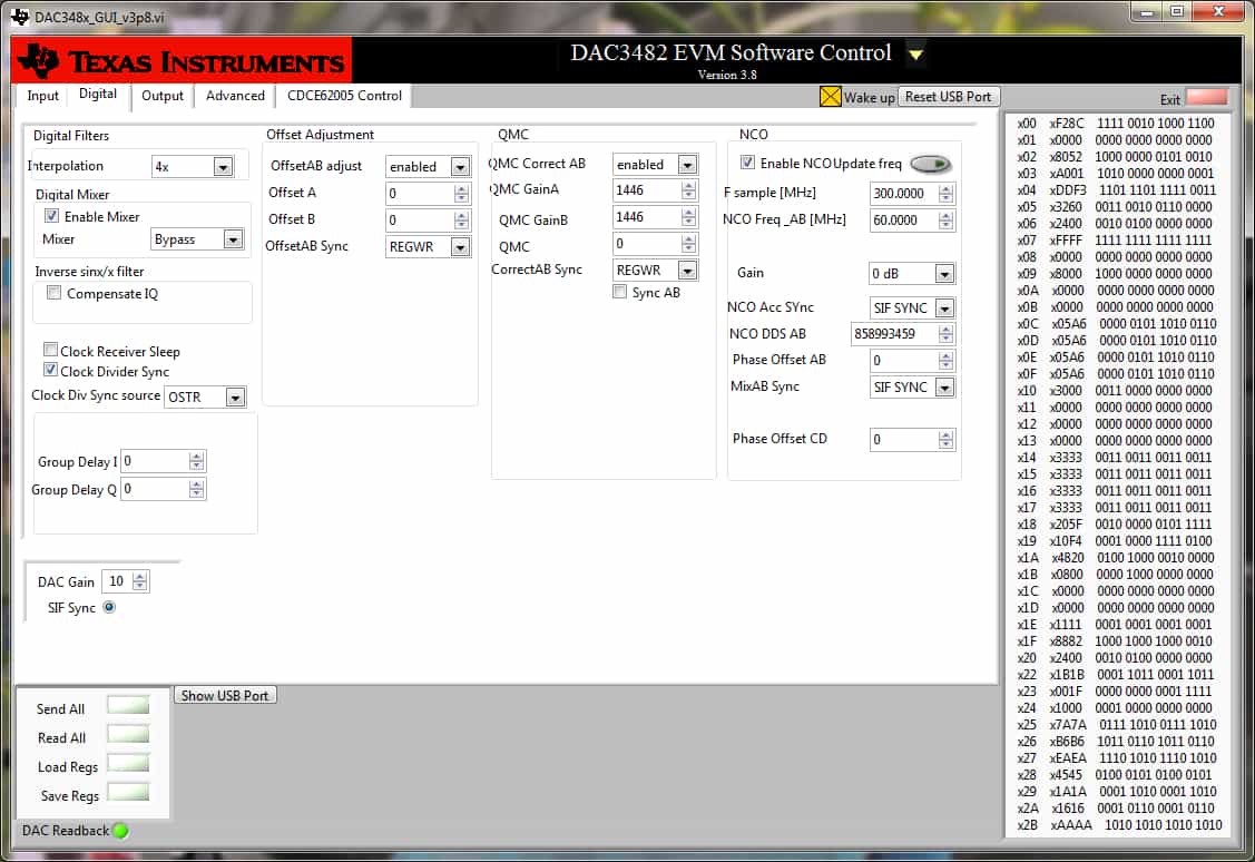
3. I would like to get those 2 signals at 2 of the outputs without any mixing between them (or any other operation between those 2 signals) at X4 interpolation. Is it possible?
I checked the datasheet and I saw that the coarse mixer can be disabled. However, I'm not sure if when the mixer is disabled, I can still do X4 interpolation?
( I noticed that the coarde mixer (CMIX) can be disabled but I cannot see how FMIX can be disabled?)
4. Is it possible to disable the NCO (Numerically Controlled Oscillators)?
I would appreciate your fast response. I must make a decision within 2 days.
Aroni,
The DAC3482 should have a DAC3482 device on it. The EVM will support both parts. That is why there is four outputs. I have your setup running in the lab. You can generate two arbitrary signals with this setup. Using the attached pattern file, I am generating a 100MHz output tone on CHB and a 50MHz tone on CHC.
You can run both outputs with x4 interpolation filter. Keep in mind that the IF signal must be =< the 0.4 x input data rate due to the BW of this filter.
You can disable the FMIX and the NCO. Writing a 0x8002 to add 0x02 will disable both. Bit 4 enables the NCO and bit 6 the FMIX.
Regards,
Jim
Aronii,
What exactly does not work? You mention "while other ones cannot be selected". What other ones are you trying to use? The TSW1406EVM should work with the DAC3482EVM up to 1.25Gsps. What rate are you testing the DAC at? Can you send screen shots of the DAC GUI? The more information you can provide the more we can help you.
Regards,
Jim
Hello Jim,
We are using those boards without extgernal clock. The jumper JP5 is with pins 2 and 3 shorted. We also selected it in the DAC3482 software.
We download a file with sine wave on one channel and DC on the other one. We connected the 2 outputs J6 and J3 directly to an oscilloscope.
We expect to see a sine wave on one channel and nothing on the other channel.
We operate the boards as follows:
1. Connect the DAC 3482 and the TSW1406 boards to USB. DAC board is connected to +6V supply as well.
2. In the DAC software we select DAC3482 on the top (black bar).
3. Then we do "Load regs" with the default file (DAC3482_FDAC_1228p8MHz_4xint_NCO_30MHz_QMCon - attached).
4. Now we change to external clock (Control -> Manual_PRI_IN we change to Manual_SEC_IN).
5. We do "Send All"
On hte TSW1406 software we do "DAC" and then select DAC3482 (on the left)
Then we download the attached CSV file. On "Data rate" we put 307.2 Mhz (we tried lower frequencies - nothing works)
and then we do SEND.
I attach all of the pictures of all screens + files + board picture (please check if jumpers are set correctly).
The CSV file was changed to TXT
Thanks for your help,
Avi
x00 xF28C x01 x0000 x02 x8052 x03 xA001 x04 x4DF1 x05 x0000 x06 x3400 x07 xFFFF x08 x0000 x09 x8000 x0A x0000 x0B x0000 x0C x05A6 x0D x05A6 x0E x05A6 x0F x05A6 x10 x3000 x11 x0000 x12 x0000 x13 x0000 x14 x0000 x15 x0640 x16 x0000 x17 x0640 x18 x205F x19 x10F4 x1A x4820 x1B x0800 x1C x0000 x1D x0000 x1E x1111 x1F x8882 x20 x2400 x22 x1B1B x23 x001F x24 x1000 x25 x7A7A x26 xB6B6 x27 xEAEA x28 x4545 x29 x1A1A x2A x1616 x2B xAAAA x2C xC6C6 x2D x0004 x2E x0000 x2F x0000 x30 x61A8 x7F x0001 CDCE62005 Registers Freq:19.200000MHz Address Data 00 80400000 01 813C0001 02 81400002 03 C10C0003 04 00040004 05 29F01A55 06 44AF0006 07 165294A7 08 20001808
Aronii,
I just verified this setup works with a TSW1406EVM and a DAC3482EVM. Please see the attached document.
Regards,
Jim
Aroni,
The onboard crystal is 19.2M and the PLL on the EVM is an integer PLL with fixed feedback divider values. Based on the crystal and the fixed feedback dividers, generating an Fdac of 1G is not possible. The closest we can get is Fdac = 983.04M which there is already a config file for this that works with the on-chip clocking option. If you need 1000M for Fdac, you will need to replace the on-board 19.2MHz, with a 20MHz crystal or something that can integer divided into 1000M. If you decide to go this route, we can assist with generating the required config file for this.
Regards,
Jim
Aronii,
Here is a brief guide on how to setup your desired configuration.
The config file for clocking the Dac at 983.04MHz is attached to this post so you should not have to change any of the settings. But just in case i included pictures of what the GUI settings should look like for you to verify that the config file works on your end.
YusufDAC3482 Internal Clock Operation.pptx
x00 xD288 x01 x0000 x02 x8052 x03 xA001 x04 xFFFF x05 x0260 x06 x2800 x07 xFFFF x08 x0000 x09 x8000 x0A x0000 x0B x0000 x0C x05A6 x0D x05A6 x0E x05A6 x0F x05A6 x10 x3000 x11 x0000 x12 x0000 x13 x0000 x14 x5555 x15 x0D05 x16 x0000 x17 x0FA0 x18 x205F x19 x10F4 x1A x4820 x1B x0800 x1C x0000 x1D x0000 x1E x1188 x1F x8882 x20 x2400 x22 x1B1B x23 x001F x24 x1000 x25 x7A7A x26 xB6B6 x27 xEAEA x28 x4545 x29 x1A1A x2A x1616 x2B xAAAA x2C xC6C6 x2D x0000 x2E x0000 x2F x0000 x30 x61A8 x7F x0004 CDCE62005 Registers Freq:19.200000MHz Address Data 00 80400000 01 811C0321 02 81400302 03 810C0303 04 00040304 05 38101A85 06 04BF1F66 07 151877F7 08 20001808
Hello,
I'm sorry fo rthe delay in my response, we were on Passover holiday + som urgent matters.
We tried your file with AD3482 software. Same file as you sent + followed your instructions. We got some weired combination of few sine waves:
However, if we do the same with DAC3484 software we get the sine waves:
As you may see nice sine waves of 50 MHz.
However, if we press this check box once again:
We get 2 sine combined waves:
So now we all understand that the hardware works but we also understand that we don't know how to operate it...
Why it does not work with DAC3482 software?
Why it is changing the waveform after we click this checkbox in DAC 3484 software?
We need to know the exact way of operating the DAC3482 boars + exact initialization because we cannot use the evaluation board fo rour project. We have to send exact parameters from FPGA.
I would appreciate your detailed answer.
REGS1.TXTHello Yusuf,
I see that you are not using the TSW1406 board as I do. I cannot define 64K complex samples as you did. Maximum samples are 32K - real or complex.
Can you take a TSW1406 board and try the same? I attach my setup file - maybe I did something wrong.
I got some sine waves now but they are 10% less than the frequency that I entered!
I enter 50 MHz - I get 45 MHz. I enter 80 MHz. and I get 72 MHz. exactly.
Can you tell me why?
One more question which was not answered:
The attached setup file is exactly the initialization of the DAC3482 registers? Is it register address + Value?