Part Number: TUSB8041A
Other Parts Discussed in Thread: TPS74801, TUSB8041EVM, , TUSB322, TUSB542
Hi all,
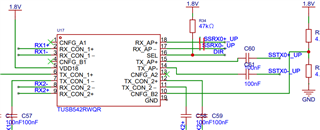
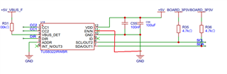
I am learning PCB design and have done a few custom ESP32 board designs successfully. I wanted to do a USB hub design and wanted some feedback on this schematic which I have attached here. Here are some of my main questions that I had on top of any feedback that you all could provide:
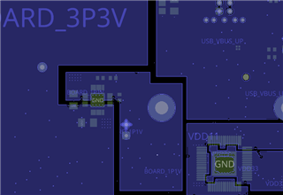
1.) I wasn't sure what the difference between VDD11/BOARD_1P1V and VDD33/BOARD_3P3V, and even BOARD_5V. Are the BOARD tags meant for traces on the PCB and VDD is meant for the power planes itself? And if this is the case, how would one generate a VDD11 plane? Would it just jump from the VDD33 and you would use an LDO or voltage divider and then you would have a BOARD_1P1V and a VDD11 plane?
2.) I wanted the USB hub to be something that functions plugged into DC5V or via a USB cable. I wanted to get any further feedback on that section
3.) At the moment I lazily generated BOARD_1P1V using a voltage divider. Could anyone recommend a more stable method of generating the BOARD_1P1V part?
Thank you for all your feedback!