This thread has been locked.

If you have a related question, please click the "Ask a related question" button in the top right corner. The newly created question will be automatically linked to this question.

HD3SS213: AUX/DDC Switch Control Logic

Expert 8760 points
Part Number: HD3SS213
Other Parts Discussed in Thread: HD3SS214, , HD3SS215

Hi team,

My customer has the following question.

-------
I am working on a project using TI HD3SS214. I refer to the following documents:
HD3SS214 datasheet, HD3SS213 datasheet and HD3SS213 EVM.

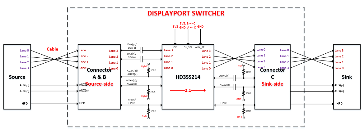
I feel confused about the AUX_SEL signal. What happen when this signal go high? 
In table 1 (page 10 - HD3SS214 datasheet and page 11 - HD3SS213) indicating AUXA
and AUXB will be high impedance, AUXC will be connected to DDC signal, but
in section 8.2.2 in HD3SS213 datasheet and table 1 - page 3 in HD3SS213 EVM say
that "when AUX_SEL = 1 the AUXB channel is routed to AUXC".

Please help me to explain this issue!
-------

I think HD3SS213 and HD3SS214 datasheet "Table 1.AUX/DDC Switch Control Logic" has the following typo.
Is this correct? Please let me know.

Best regards,
Fumio Nakano

  • Fumio-san

    Please follow the table, the description in section 8.2.2 is not correct and needs to be fixed.

    Thanks
    David
  • you may right, let's check with system guy
  • Hi David-san, Brian-san,

    Thank you for your quick reply.

    I will wait for your check result.

    Best regards,
    Fumio Nakano

  • Fumio-san

    I confirmed that the table is correct, the description is a typo and needs to be updated.

    Thanks
    David
  • Hi David-san,

    Thank you for your check.

    But, sorry my correction was wrong.

    My customer pointed out my correction error.

    Please read below.

    -----------------------------------------------------------------------

    Thank you for your response.

    But according to your correction, the Dx_SEL signal will have 3 configurations: L, H and M,

    while AUX_SEL only has 2 configurations: L and H. That conflicts with the rest of the datasheets

    and the schematic is shown below (HD3SS213 EVM):

    image.png

    :

    Please check it again and let me know as soon as possible.

    -------------------------------------------------------

    I think that the table should be corrected as follows.
    Please check it again.


    Best regards,
    Fumio Nakano

  • Fumio-san

    The table is correct. The description in section 8.2.2 needs to be updated.

    AUX channel is controlled by AUX_SEL and DX_SEL. These two pins configure the switch to route the incoming AUX signal to the outgoing AUX path, when AUX_SEL = 0 and DX_SEL = 0, the AUXA channel is routed to AUXC, when AUX_SEL = 0 and DX_SEL = 1, the AUXB channel is routed to AUXC.

    Thanks
    David

  • Hi David,

    How about the Table 1. HD3SS213 EVM Jumper Description and Settings (in the HD3SS213 EVM)? Does it also need to be updated?

    Thanks,
    Hai
  • Hai

    AUXSEL jumper definition needs to be expanded for more detail in the EVM user guide. But please refer to table 1 of the HD3SS213 datasheet for the correct mapping of switch control logic.

    Thanks
    David
  • Hi David-san,

    Thank you!!

    Best regards,
    Fumio Nakano
  • Hi David,

    Thank you very much for your support.

    I have another question about pull-up resistors for DDC signal.

    Let see the schematic below:

    I have read the datasheet of TDMS181 and HD3SS215 for the HDMI application,

    but I have a problem about the value of pull up resistors for DDC clock and data.

    Could you tell the value of R1 to R10?

    Thanks and best regards,

    Hai

  • Hai

    Same question has been addressed in this e2e thread: e2e.ti.com/.../737162.

    Thanks
    David
  • Hi David,

    Thank you so much for your support.

    Sorry to bother you, but I have another question.

    I wonder if the HD3SS214 can be used to switch from one of two sources to one sink and one source to one of two sinks

    in one application by using some control pins, as shown below:

    Fig.1. Control pins for HD3SS214 switching

    For switching from one of two sources to one sink, the configuration as shown in Fig 2.

    Fig.2. 2:1 Application for HD3SS214

    And for switching from one source to one of two sinks, see Fig 3.

    Fig.3. 1:2 Application for HD3SS214

    Can I do that? 

    Thanks and best regards,
    Hai

  • Hai

    The DP source and sink receptacles have complete different pinout. I don't see how you can use the same receptacle to serve two different purposes.

    Thanks
    David
  • Hi David,

    Thank you for pointing out my problem.

    Then I modified the configuration. Let's see two figures below:


    Based on this configuration, the displayport switcher does not change to serve two different purposes.

    I think it just the name of the Lanes are replaced (ex: Lane 0 instead of Lane 3, Lane 1 instead of Lane 2, ...),

    but the trace will not change. It only needs the crossover trace between the HD3SS214 and the Connector C.

    Is it right?

    Thanks & Best Regards,

    Hai

  • Hai

    You need to make sure the lane ordering is correct when going from the source to the sink.

    Thanks
    David
  • Hi David,

    I follow this image for lane ordering. I make the DP switcher look like a cable.

    Then the source will connect to the sink through 3 cables (source => cable 1 => switcher (Cable 2) => cable 3 => Sink)

    It is the same as connecting through 1 cable. Thus, the order of lane will not change.

    Beyond the lane ordering, is there any other problem when using the HD3SS214 to serve two different purposes?

    Thanks and best regards,

    Hai

  • Hai

    HD3SS214 supports 2:1 and 1:2 DP differential switch. Because it is a switch, it does not have any equalizer or re-driving capability, please make sure the sink can support the total loss of 2 cables plus HD3SS214.

    Thanks
    David
  • Hi David,

    Thank you for reminding me. I will carefully consider this issue.

    Thanks and best regards,

    Hai