This thread has been locked.

If you have a related question, please click the "Ask a related question" button in the top right corner. The newly created question will be automatically linked to this question.

MCU-PLUS-SDK-AM263X: Startup instability in UART TX data

Part Number: MCU-PLUS-SDK-AM263X
Other Parts Discussed in Thread: AM2634, SYSCONFIG

Hi

We have designed a MCU(AM2634) +PMIC (TPS653850) board but I am facing a startup issue problem when I add all GPIOs in my final design (about 84 GPIOs) to the "hello world" example code.

Problem Description:

  • I have used “hello_world_am263x-cc_r5fss0-0_freertos_ti-arm-clang” example from “AM263x MCU+ SDK  09.00.00” as the base software and added 84 GPIOs to the syscfg file. Only one of these 84 IOs is used as LED and remaining 83 IOs are only initialized in the Sysconfig generated files and never used in the main code.
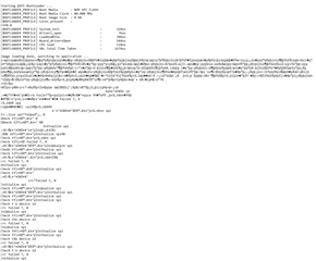
  • The problem arises when the board is powered up after being off for a while, the MCU sends garbage to the UART console and it takes time (about 15 seconds) to be fixed and normal data is received on UART. After stablization if the board is turned off and powered up again without significant delay it works fine without problem. Otherwise, if it is off long time the garbages come again.
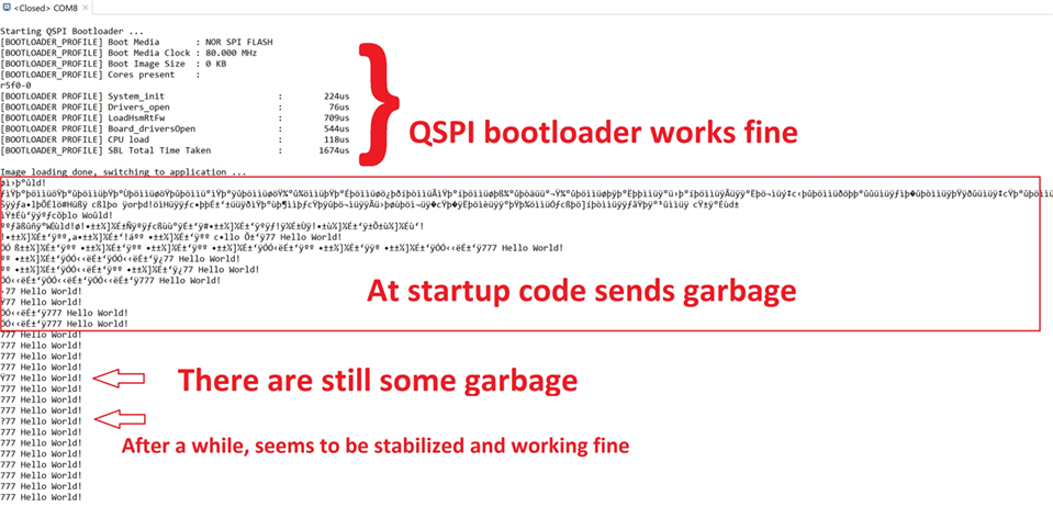
UART TX data during instability

  • The duration of being off has direct relation to the time that the board takes to be stabilized and working fine.
  • An important point to mention is that the same code works completely fine in AM263x Control Card EVM.
  • Hi Saman,

    My guess is that there are some pinmux conflicts among the UART pins and the 84 GPIO pins you added. Can you do the same for the hello_world_am263x-lp_r5fss0-0_freertos_ti-arm-clang instead of the AM263x CC hello world example? Make sure the A7 and A6 are not used in your 84 GPIO pins. 

    Best regards,

    Ming

  • Hi Ming,

    First of all, I should mention that UART pins B5,A3 are used as debugging port in my hardware instead of A7/A6.

    Secondly, there are no conflicts in GPIOs and Other ports. I have checked it and if there were some conflict, SysConfig also gives automatic error.

    May I ask  what is the point of using LP example instead of CC example?

    BR

    Saman

  • Hi again,

    When I debug, exactly after pin_mux_init function these bad behavior appears.

  • Hi 

    I tested also with LP-hello world example. the result is same

  • Hi Saman,

    I forwarded this thread to our HW app team for further help.

    Best regards,

    Ming

  • Hello Saman,

    We recommend including series termination near the AM263x transmitter for UART transmit signals. Series termination resistors are placed in order to control rise-time and reflections of data lines. The value of the resistor will vary based on the PCB layout and may range between 0 to 40Ω.

    Would it be possible to swap R3916 with a 33Ω resistor to see if that solves the issue? If not, we can continue trying to root cause this issue. 

    Also, you mentioned that this example works with the AM263x Control Card. To be clear, it worked with all GPIOs added as described in your problem statement, correct? 

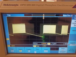
    In the screenshot of the SPI clock signal, which ball was being configure for SPI CLK to measure this waveform? It should also be noted that we recommend a series termination resistor for SPI clock signals as well at the AM263x transmitter. 

    Regards,

    Erik

  • Hello Erik,

    Would it be possible to swap R3916 with a 33Ω resistor to see if that solves the issue?

    I will change R3916 and come back to you.

    Also, you mentioned that this example works with the AM263x Control Card. To be clear, it worked with all GPIOs added as described in your problem statement, correct? 

    Yes, the example code with GPIOs added works with AM263x Control Card.

    In the screenshot of the SPI clock signal, which ball was being configure for SPI CLK to measure this waveform?

    SPI1_CLK (A10) is used for clock.

    It should also be noted that we recommend a series termination resistor for SPI clock signals as well at the AM263x transmitter. 

    As it can be seen in schematic R2220 is used as series resistor.

    By the way, please note that this instability ONLY occurs during first 30 seconds of the board power up if the board had been off for a while.

    I mean that it seems that something is charging/discharging as the time passes.

    BR

    Saman

  • Hello Saman, 

    Please let me know if the swap affects the results. I am checking internally for any other potential causes to this issue.

    Regards,

    Erik

  • Hi Erik,

    I replaced the R3916 with 33R resistor. But it did not resolve the problem. 


    Do you have any feedback from your side?

    I should mention again that this problem is only pops up at startup and only when the MCU had been in reset mode (either power OFF or PORz in low state) for a while. And after MCU works for a few seconds the instability in UART-TX and SPI Clock and SPI CS will disappear.

     And again I should mention that this problem as you can see in the picture below does not pop up in RBL and SBL and when the core switches to the main application with 84 GPIO, the problem arises.

    BR 

    Saman

  • Saman, 

    It is hard for me to debug this issue since it can't be replicated on the AM263x Control Card EVM. I ran your same appimage for the EVM and saw the same correct behavior.

    Based on the SPI CLK signal scope shot, it seems like there is something else that is driving the clock signal. I could not see anything from the schematic. Can you confirm that there is nothing else driving the line? 

    Also, to test, can you add a vTaskDelay() before the while loop in your code and see if that has any impact. 

    Did you make any other changes to the default_sbl_qspi.cfg other than the file destination? 

    Can you try configuring a GPIO (try with A10 and B5 and other pins that you are observing issues on) LOW immediately within your application code and see if it is driven high? Could you send a scope shot that triggers on PORz and shows how the GPIO is driven?

    Can you confirm that the power sequencing is coming up as expected? 

    Regards,

    Erik

  • Hello Erik,

    I ran your same appimage for the EVM and saw the same correct behavior.

    That's correct. I should emphasize that I tested the code on EVM and it worked fine. so it doesn't seem to be a software issue.

    Based on the SPI CLK signal scope shot, it seems like there is something else that is driving the clock signal. I could not see anything from the schematic. Can you confirm that there is nothing else driving the line? 

    No nothing else is driving the line. Please not that this problem is not only for the SPI_CLK. I can see similar problem in the waveform of the other pins like UART_TX and other GPIOs (I tested also on LED pin)

    Also, to test, can you add a vTaskDelay() before the while loop in your code and see if that has any impact. 

    No impact

    Did you make any other changes to the default_sbl_qspi.cfg other than the file destination? 

    I think this is not the case. but I have changed device id in order to match with the FLASH device on my board.

    Can you try configuring a GPIO (try with A10 and B5 and other pins that you are observing issues on) LOW immediately within your application code and see if it is driven high? Could you send a scope shot that triggers on PORz and shows how the GPIO is driven?

    I have also tested by toggling only one GPIO in a loop. but the result was same. I mean that the pin could not easily de-asserted (going low) in first moments of the MCU powered on.

    Can you confirm that the power sequencing is coming up as expected?

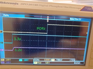
    Here is also the power sequence of the board.

    By the way,

    I need to test the board with internal oscillator in order to avoid any potential Mis-functionality which can be produced from external crystal.

    I changed  the input clock source to SYS_CLK. but the result was same and the problem was still there.

    Is that the correct way of using internal oscillator?

    BR

    Saman

  • Hi Saman,

    Thank you very much for the detailed reply and all the details.

    Can we please do few of the checks below?

    1. The debugger for UART that you are using, can you please check once if the voltage levels of the debugger are compatible with AM263x? If possible, can you take the same Oscilloscope shots once without the debugger connected to CN3901?
    2. Just few things I noticed in the schematic,
      1. The Crystal XTAL3200(DSX321G) has a series 1.8kohm resistor R3203, is that intentional?
      2. The series termination resistor R3915 on the UART0_TXD must be close to AM263x in layout. I don't see this to be causing any problem, but just a good practice.
    3. Is there any other board connected to this board? If possible, can you try disconnecting those boards and trying this once? Since I see this board has CN1 and CN2 connectors and the power rails are also on CN1 and CN2.
    4. Also, when you tried the same code on AM263x Control Card, did you change the debug UART from UART2(B5, A3) to UART0(A7, A6)?
    5. Also is this observed only on one board or is it observed on multiple boards?

    Please let me know about these.


    Thanks,

    Tejas Kulakarni

  • Hi Tejas,

    The debugger for UART that you are using, can you please check once if the voltage levels of the debugger are compatible with AM263x?

    The debugger I am using is XDS110-USB and I think that it is compatible with AM263x.

    If possible, can you take the same Oscilloscope shots once without the debugger connected to CN3901?

    Yes I will send it asap.

    The Crystal XTAL3200(DSX321G) has a series 1.8kohm resistor R3203, is that intentional?

    This series resistor is intentional but the value might be revised based on the XTAL-I characteristic.

    The series termination resistor R3915 on the UART0_TXD must be close to AM263x in layout

    No it is not so close to the MCU. but I do not think that this is an issue in our case.

    Is there any other board connected to this board? If possible, can you try disconnecting those boards and trying this once? Since I see this board has CN1 and CN2 connectors and the power rails are also on CN1 and CN2.

    No. at the moment no board is connected to CN1 and CN2. and the power is sourced by soldering a wire to the board.

    Also, when you tried the same code on AM263x Control Card, did you change the debug UART from UART2(B5, A3) to UART0(A7, A6)?

    Yes. the only difference between two codes is this change of the UART port.

    But please consider that this problem is not limited only to the UART data. and I have the same issue in the waveform for SPI_CLK and any other GPIOs. so I guess that the source of the problem is an hardware issue or something inside the MCU at startup.

    BR

    Saman

  • The Crystal XTAL3200(DSX321G) has a series 1.8kohm resistor R3203, is that intentional?

    Hi Tejas,

    Do you have any recommendation of changing this resistor? or removing it?

    Saman

  • Hi Saman,

    Thank you again for your replies.

    I would recommend keeping R3203 as 0Ω and gradually change based on further testing. In AM263x datasheet section 7.11.4.1.1 we recommend a Crystal Effective Series Resistance max of 46Ω. So please change this to 0Ω and let us know if it solves the observation.

    Also, can you please let us know if you are seeing this observation in multiple boards, or is this in one board only?

    Thanks,
    Tejas Kulakarni

  • Hi Tejas,

    OK I will do those and let you know the result.

    But before that I am going to run the MCU with internal oscillator.

    So I set the Input clock source as RCCLK10M. Is that correct? should I do something more?

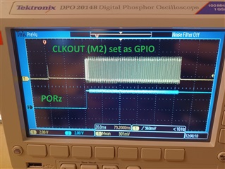
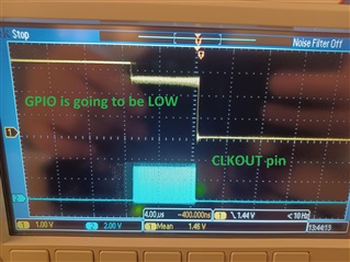
    One more point is that I checked the CLKOUT pin (M2) with oscilloscope. and here is the photo of that at the early seconds of the power up (about first 30 seconds) during instability. Is it supposed to be like this?

    After that period of instability the CLKOUT will be fine and oscillates continously at 25Mhz.

    BR

    Saman

  • Hi Saman,

    For running the MCU with internal RC Oscillator, we will get you more details.

    On the CLKOUT, can you please probe the CLKOUT and also one toggling GPIO is possible with respect to PORz so that we can see at what points after PORz this behavior is seen.

    Please do let us know about the change in the R3203 to 0Ω and its observations.

    Thanks
    Tejas Kulakarni

  • Hey Saman,

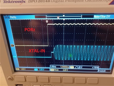
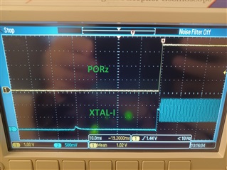
    I got notified of a video(e2e.ti.com/.../4_5F00_5989972961090605679.mp4) that you attached to this thread. Looking at it, I am assuming the below.

    Channel 1 - GPIO
    Channel 2 - XTAL Crystal Clock
    Channel 3 - PORz

    From that it looks like the XTAL Crystal Clock is NOT stable/clean? Also looks like there is too much Jitter on the clock? Sorry but could not see much clearly in the video. 

    Did you check the same by changing R3203 to 0Ω? And also, if it is clear that the XTAL Crystal Clock is not clean, can you change the crystal component (XTAL3200) once to a new/different component and try once? Please try these if possible and let us know.

    Also please let us know if this is occurring on only one board or multiple boards?

    Thanks,
    Tejas Kulakarni

  • Hi Tejas,

    Thanks for giving details on internal RC oscillator. I am looking forward to that.

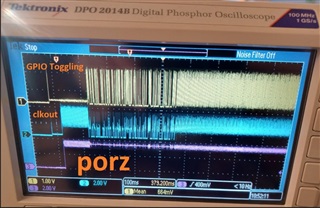
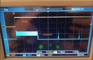
    Here is the scope shot of the signals you requested. you can see that in the first 100ms when the GPIOs are not initialized in pin_mux_init, the clkout seems to be fine but after that for about few hundred milli seconds both clkout and GPIO are not working properly. This time could be increased to about 30 seconds if the board has been off for longer time.

    Here you can see the clkout signal vs PORz on the board which has been off for longer time.

    Here you can see the clkout (Blue) and toggling GPIO(yellow) and PORz (pink) at startup.

    For the R3203, I have contacted to crystal manufacturer to get more information about it.

    BR

    Saman

  • Hi Tejas,

    From that it looks like the XTAL Crystal Clock is NOT stable/clean? Also looks like there is too much Jitter on the clock? Sorry but could not see much clearly in the video.

    Yes there is much jitter on the clkout pin as it can be seen in the video and photos.

    Did you check the same by changing R3203 to 0Ω? And also, if it is clear that the XTAL Crystal Clock is not clean, can you change the crystal component (XTAL3200) once to a new/different component and try once? Please try these if possible and let us know.

    Regarding R3203, 1.8K is the suggestion of the crystal manufacturer. so I am discussing with them to get any suggestion. and if it is fine to have 0ohm for that.

    Also please let us know if this is occurring on only one board or multiple boards?

    Yes it is same in the second board as well.

    If you can help me to enable internal Oscillator I can verify that the issue is with external crystal.

    Should I disconnect R3203 when I try to have internal oscillator in the MCU?

    BR

    Saman

  • Hi Saman,

    Please refer to Section 3.1 of AM263x and AM263Px Hardware Design Guidelines (Rev. B) for details on how to connect external single ended clock.

    For connecting single ended clock, you would have to disconnect R3204 to make XTAL_XO floating and connect clock to XTAL_XI as per the above document. Hope the PCB has provision to provide external clock with proper clock integrity.

    I will ask our team to provide details on how to enable internal clock, but I do not expect that to solve the observation, since the initial boot would always happen with the External clock connected to XTAL pins. Since this observation is occurring during the initial few seconds of boot, it would always persist until this clock integrity is fixed would be my guess. So, I would suggest to fix the crystal clock integrity on priority.

    Thanks,
    Tejas Kulakarni

  • Hi Tejas,

    I changed the R3203 to 0 ohm but it did not resolve the problem. Can you consult with team and guide me since I do not have any clue of how to resolve the problem.

    BR

    Saman

  • Hi Saman, 

    We need to look at the schematic and layout of this design to debug further. Can you coordinate with your local field support?

    Thank you,

    -Randy

  • Hello Saman, 

    In looking at the CCS project again, I noticed that although the GPIO are only initialized, they are configured as outputs. Therefore, all GPIO configured as outputs would be driven low at startup. Would you be able to test if there is the same instability if all GPIO are configured as Input for the PIN direction?

    Also, for the GPIO that are initialized as outputs, can you confirm if any are connected to large capacitive loads? If there are multiple large capacitive loads during the startup with many GPIO outputs being driven, the current limit of the I/O may be exceeded during the "startup time". 

    If you are able to confirm that the GPIO being configured as inputs works, then a potential workaround would be to use GPIO_setDirMode() to configure desired GPIO as output after a delay. 

    Regards,

    Erik

  • Hi Erik,

    Even with all GPIOs set as input the problem is there.

    I reduced the number of GPIO to 10 then I noticed that although  the problem is resolved but the shape of the CLKOUT pin (M2) is not ideal like when the MCU is in NO-Boot Mode. (which is square wave with 50% duty cycle)

    But when I increase the number of GPIO to 30, (Even as Input) the problem pops up

    BR

    Saman

  • The point which is important here is that the number of GPIOs is important not the specific GPIO which is added

  • Hi Saman, 

    Thanks for the additional layout info - I'll review that today.

    The basic failure signature (from your above UART TX post) looks to be like some kind of bus contention issue, but we cannot replicate that yet with your CCS project files on our EVM. We'll try looking at other UART and CLKOUT signals as well - but it doesn't seem to effect our default UART port on the EVM. 

    Although the problem seems to track NUMBER of IOMUX pads configured as GPIO, I wonder if there might be a specific group or even specific pin in that larger set that is causing this. 

    Then on the PORZ scope shot you linked as well, that looks like what might be a power integrity issue on the common 3.3V I/O rail. The oscillation on the PORZ pin (around +/-200mV it looks like?) shouldn't be enough to cause any kind of reset issue, but it does indicate that you might be exceeding the VDDS33 datasheet limits (3.135V to 3.465V) on this board and therefore also the VDDA33 limits. The VDDS33 is used internally to power the VDDS18 and VDDA18 on-die LDO - that would further effect I/O and oscillator performance if those 1.8V LDO input requirements are not satisfied. Can you take a closer look at 3.3V transients before/during failure state?

    Thank you,

    -Randy

  • Hi Randy,

    I wonder if there might be a specific group or even specific pin in that larger set that is causing this. 

    As far as I tested, it does not seem to be related to the specific IO and it only relates to the number of GPIOs initialized in the firmware.

    The oscillation on the PORZ pin (around +/-200mV it looks like?) shouldn't be enough to cause any kind of reset issue, but it does indicate that you might be exceeding the VDDS33 datasheet limits (3.135V to 3.465V) on this board

    That oscillation on the PORz is the problem in measurement maybe caused by the improper probe GND connected and caused by the other probe (blue one) signal. Since I cannot see that oscillation when the blue probe is not connected. here is a shot with better quality measurement:

    The point that I have understood so far is that so long as we don't have proper oscillation on CLKOUT (M2) pin, we cannot have proper firmware operation. and the major problem that I experienced is that the MCU cannot easily drive pins to low.

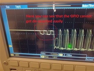
    here is another scope shot of a code toggling one GPIO (although there are other 69 GPIOs initialized as input but never used in the firmware). you can see that the GPIO cannot easily de-asserted and takes time to goes low.

    Please be aware that the noise on the yellow signal is caused from blue probe signal and will be removed if I disconnect blue probe.

    Would you please let me know that how CLKOUT pin is driven and how the signal on the CLKOUT pin is generated?

    And also please note that if I only add one GPIO toggling in the sysconfig I won't have any problem in the firmware nor on the CLKOUT signal.

    BR

    Saman

  • Hello Saman,

    In your project, you have M2 configured as a GPIO. When the application code is run, the muxmode of M2 is configure to mode 7 for GPOI138. Therefore, what you are observing is expected behavior in terms of the CLKOUT0 pin going low indefinitely (output driven low). In order to observe CLKOUT0 normally during the application code, you will need to change GPIO allocated for M2 to be on a different ball. When you have done this, you will be able to see the 25MHz clock reflected on CLKOUT0 by default. 

    Would you please let me know that how CLKOUT pin is driven and how the signal on the CLKOUT pin is generated?

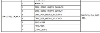
    CLKOUT0 is generated by a General Clock Mux choosing a clock source. The default is XTALCLK (25MHz Crystal input). The clock mux modes for CLKOUT0 are detailed here: 

    To change the output configuration of CLKOUT0, then you will need to write to the following registers:

    • TOP_RCM_CLKOUT0_CLK_SRC_SEL (0x53200C00)
      • Responsible for selecting the clock source
      • Clock source mode <N> should be loaded into the register as multibit (0xNNN)
      • For example, if you want to select RCCLK10M, then you would write 0x00000555
    • TOP_RCM_CLKOUT0_CLK_DIV_VAL (0x53200C08)
      • Responsible for dividing the clock source 
      • The divider value results in the output being (clock source)/(N + 1) where N is the value written to the DIV_VAL register
      • Divider value N should be loaded into the register as multibit (0xNNN)
      • For example, if you want to divide by 4, then you would write 0x00000333
    • TOP_RCM_CLKOUT0_CLK_GATE (0x53200C10)
      • Responsible for gating the output
      • By default, CLKOUT0 is ungated and will output configured clock source
      • To gate the output, write 0x00000007
      • To ungate the output, write 0x00000000

    The CLKOUT0 status will be represented in the TOP_RCM_CLKOUT0_CLK_STATUS (0x53200C18) register.

    • Bits 0:7 represent the clock source selected 
      • Clock source mode is assigned to the associated bit 
      • For example, RCCLK10M is mode 5 and so bit 5 is set (0x20)
    • Bits 8:15 represent the current divider value of the clock source
    • For example, if CLKOUT0 is configured to be RCCLK10M divided by 10 then the STATUS register would read 0x920
    And also please note that if I only add one GPIO toggling in the sysconfig I won't have any problem in the firmware nor on the CLKOUT signal.

    Can you please elaborate on this? When you only have one GPIO, my expectation would be that you have CLKOUT0 reflecting the 25MHz frequency indefinitely. Is this what you observe? 

    Please note, in the image below, CLKOUT oscillating at 25MHz represents the time between PORz assertion and the application code running since the application code configures M2 to be a GPIO.

    With this in mind, could you please run a series of tests for me on the custom HW? If the time duration that CLKOUT0 is 25MHz represents the instability time (we can call this T_startup), can you try running the application under the following conditions:

    • with only two GPIO added in SYSCONFIG (LED_GPIO and CLKOUT0 (M2) GPIO) 
    • with 20 GPIO added in SYSCONFIG (LED_GPIO, CLKOUT0, and 18 GPIO)
    • with 40 GPIO added in SYSCONFIG (LED_GPIO, CLKOUT0, and 38 GPIO)
    • with 60 GPIO added in SYSCONFIG (LED_GPIO, CLKOUT0, and 58 GPIO)
    • with 80 GPIO added in SYSCONFIG (LED_GPIO, CLKOUT0, and 78 GPIO)

    For each configuration, please take a scope shot of PORz and CLKOUT pin as well as record the T_startup (time that the 25MHz frequency oscillates on the CLKOUT pin). 

    We are still reviewing the layout and other provided material to try and identify the root cause. 

    Regards,

    Erik 

  • Hi Erik,

    In your project, you have M2 configured as a GPIO. When the application code is run, the muxmode of M2 is configure to mode 7 for GPOI138.

    Yes you are right, this project was uploaded in the first days of the problem when I used CLKOUT0 as GPIO. But, later I removed CLKOUT0 assignment as GPIO and the CLKOUT0 behavior (Instability at startup) that I attached is for the time that CLKOUT0 (M2) is not assigned to any GPIO in SYSCONFIG.

    Please note, in the image below, CLKOUT oscillating at 25MHz represents the time between PORz assertion and the application code running since the application code configures M2 to be a GPIO.

    No that's not correct since M2 is not configured as GPIO as I mentioned above. In the picture it can be seen that GPIO there is a transient part in de-assertion of the GPIO in which the GPIO is not completely low. (This behavior was seen in UART-TX and SPICLK before)

    Can you please elaborate on this? When you only have one GPIO, my expectation would be that you have CLKOUT0 reflecting the 25MHz frequency indefinitely. Is this what you observe? 

    Yes exactly.

    • with only two GPIO added in SYSCONFIG (LED_GPIO and CLKOUT0 (M2) GPIO) 
    • with 20 GPIO added in SYSCONFIG (LED_GPIO, CLKOUT0, and 18 GPIO)
    • with 40 GPIO added in SYSCONFIG (LED_GPIO, CLKOUT0, and 38 GPIO)
    • with 60 GPIO added in SYSCONFIG (LED_GPIO, CLKOUT0, and 58 GPIO)
    • with 80 GPIO added in SYSCONFIG (LED_GPIO, CLKOUT0, and 78 GPIO)

    Do you want me to assign M2 pin as GPIO?

    I will prepare the scope shots you requested and send you later.

    By the way,

    Since I am suspicious about the XTAL input. I really want to use the internal oscillator to check the problem. I have set the "Input Clock Source" as RCCLK10M in the SYSCONFIG. but I did not see any difference. could you please help me regarding this also?

    BR

    Saman

  • Hi Erik

    Here is the scope shot of the PORz vs CLKOUT (assigned as GPIO) which is for all cases you requested.

    But please note that when CLKOUT is not assigned to any GPIO the waveform of the CLKOUT would be different in different cases which you requested.

    With GPIOs less than 20 (including 20), CLKOUT shape is almost good (25Mhz square waveform)

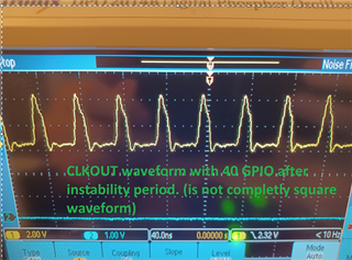
    With GPIOs 40, CLKOUT has instability at startup and even after startup the waveform of the CLKOUT is not as good as before (clean square waveform)

    With GPIOs 80, the CLKOUT never stabilizes, and toggling GPIO LED cannot easily and immediately drives low. as can be seen in the picture below.

    I hope that I could explain clearly about the situation. please ask if there is something unclear.

    BR

    Saman

  • Hello Saman,

    I am reviewing internally to try and diagnose the root cause. 

    • Is this issue unique to single board or all custom boards affected? 
    • What is the device revision? A, B, or C?

    Regards,

    Erik

  • Hello Erik,

    Is this issue unique to single board or all custom boards affected? 

    There are 2 custom sample boards soldered. And, both of them have the same problem.

    What is the device revision? A, B, or C?

    The revision on both boards is 'B'.

    BR

    Saman

  • Hello Saman,

    I was able to find an old Control Card with the device Revision, B and found that it also worked (no instability time) with the example app image that you originally sent over. 

    Would it be possible to try and use an SR1.1 device (revision value: C) with your custom hardware to rule that out as a variable? 

    Regards,

    Erik

  • Hi Erik,

    I had tested the code on TI EVM CC here with revision B before and it was working fine here also.

    Unfortunately, at the moment I do not have revision C chip to solder it on our custom board.

    BR

    Saman

  • Hi TI team,

    I found something in our schematic that might be the source of the problem

    The VDDS18s are not connected to T3.

    Would you please guide if there is any possibility to connect them internally? if yes how?

    Since I don't have the access to those VDDS18s pins on the board, would you please tell me if I cannot connect them internally, what would be the effects of this mistake and is it directly related to our issue?

    Another issue that I found is that VSYS_MON is connected to a resistor voltage divider in the TI EVM boards but in our custom board it is connected to DGND. Would you please tell me if that would cause any problem?

    One more question about the TI EVMs,

    I checked the LP and CC EVM schematics, In the CC, the T4 pin (RSVD_T4) is connected to GND according to the datasheet, but surprisingly T4 pin is connected to 1.2V in LP schematic.

    Can you explain why?

    BR

    Saman

  • Saman,

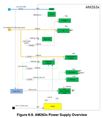
    VDDS18_LDO not being connected to the VDDS18 power pins is most likely the root cause of the observed issues. I am sorry that I did not catch this in my initial review of the schematic. VDDS18 is the 1.8V IO Bias supply and it must be connected externally to the VDDS18_LDO output. There is no way to connect this internally. For more details, please refer to Chapter 6.2.1 "Power Management Overview" of the AM263x TRM. 

    Since you had the VDDA18_LDO supply pins connected to the VDDA18 supply pins, there would be no issues with the reset sequence (as you observed) as there is no check on the VDDS18 supply as a part of the sequence. There is a POK that can be configured to monitor the VDDS18 supply but this would not be helpful since it would always flag undervoltage due to the power pins left floating.  

    The problem however is that the IO requires the VDDS18 supply and as more were added and configured/initialized the more the issue with not having the 1.8V IO Bias supply was apparent. There is likely some backchanneling that is charging the VDDS18 supply which is why, after some time, there is "normal" operation. 

    Despite the observation that the IO works after an "instability time", it is highly recommended that the board be redesigned with the VDDS18_LDO output tied to the VDDS18 power supply pins. If there is some way to modify the board to connect the LDO output to the VDDS18 power net then that would correct this issue but you mentioned that the power net is not accessible on this board. 

    I checked the LP and CC EVM schematics, In the CC, the T4 pin (RSVD_T4) is connected to GND according to the datasheet, but surprisingly T4 pin is connected to 1.2V in LP schematic.

    The T4 pin was connected to 1.2V for internal use, on custom designs it should be connected to ground. RSVD_U1 should also be connected to ground. 

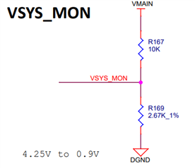
    Another issue that I found is that VSYS_MON is connected to a resistor voltage divider in the TI EVM boards but in our custom board it is connected to DGND. Would you please tell me if that would cause any problem?

    The VSYS_MON is an optional feature and by default will not affect the functionality of the device. The VSYS_MON is a 0.9V comparator that can be used to monitor the system voltage. A voltage divider should be used to divide down the system voltage (or any supply that is of interest to be monitored) such that the lower tolerance of the supply equates to 0.9V. For example, if you wanted to monitor the 5V rail for when the voltage is below 15% threshold (4.25V)  then you would use a voltage divider such as the one in the Control Card design: 

    This way, when the 5V supply is below 4.25V then the POK module will flag and an interrupt can be used to take action. 

    Please let me know if you have any additional questions.

    Regards,

    Erik