The TI E2E™ design support forums will undergo maintenance from July 11 to July 13. If you need design support during this time, open a new support request with our customer support center.

This thread has been locked.

If you have a related question, please click the "Ask a related question" button in the top right corner. The newly created question will be automatically linked to this question.

kindly check the circuit diagram of auto phase selector switch

Other Parts Discussed in Thread: LM358, TLV2333, TINA-TI, LMV358A

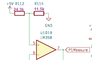
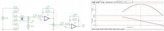
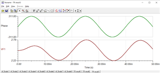
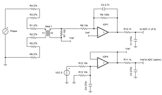
hello, I have attached herewith circuit diagram of auto phase selector. so kindly check and update as to any corrections required in this circuit??? as this is going to be used commercially and this is analog part of the circuit. microcontroller part, program I will post later for any corrections. here in this product, microcontroller will sense incoming input voltages of all three phases individually and choose best phase among three (around 220v AC) for the output load. here as I said, I am asking you to check only analog part. mcu part I will post later for any correction

   auto phase selector.pdf   

  • Hello Atish,

    Welcome to the e2e forums.

    The high pass filters (10k 1uF) are set to 16Hz so only -0.4dB signal loss at 50Hz

    LM358 is not rail to rail output so the center voltage of 2.5V will clip on the high side well before the low side. Earlier high clip at low temperature.  More dynamic range of VOUT will occur with a center about 1.6V 

    Only one voltage divider is needed for all pin 5, if combined add a capacitor to ground. 

  • 1. The high pass filters (10k 1uF) are set to 16Hz so only -0.4dB signal loss at 50Hz- so possible correction here will be what???

    2. LM358 is not rail to rail output so the center voltage of 2.5V will clip on the high side well before the low side. Earlier high clip at low temperature.  More dynamic range of VOUT will occur with a center about 1.6V - so here what modification is to be done in the LM358 part for the best outcome???

    3. Only one voltage divider is needed for all pin 5, if combined add a capacitor to ground. -  I think only one voltage divider is only there at pin 5 of LM358 for each respective phase. kindly check and confirm

    4. with 10k variable resistor at pin 1 of LM358, what functionality, can we achieve???

    any other modification for the best performance????

  • also, precision dc rectifier chip needed????

  • instead of lm358, kindly suggest high precision opamp for accurately measurement and sensing ac input voltage for MCU to read

  • Atish,

    1) Increase capacitance or increase resistance to lower HPF cutoff frequency, if the 4.3% signal attenuation is unacceptable.

    2) 

    3) Are the three op amps close to each other on the board? If yes, then there is a chance to reduce resistor count. 

    4) This pot changes gain from 0 to 100.

    5) Do you want to know live value for phase voltage (as is). Do you want the peak voltage? if yes, then rectifier needed. Do you want average voltage? If yes, then half or full wave rectification followed by low pass filer much lower than 50Hz is needed. Do you want true RMS voltage? If, yes that'll be much harder.

    6) Depending on "5", I can suggest an alternative. 

  • here ideal phase voltage is 220v AC which is usually RMS value. so here in our project, there will be 3 phases which need to be measured and sensed accurately and must be read by mcu to take correct decision on which phase is best and choose that for the connected single phase load for uninterrupted operation in real time.

    so, in place of LM358, any other high precison opamp can you suggest or what if we use IC similar like BL0942 (available in china, not available in India) or sensor IC like stpms2l-pu' or similar (part must be available in Indian market) for higher accuracy and better performance???? so kindly suggest best chip for LM358 replacement and that component must be available in Indian market

    precision DC rectification part will be needed in our circuit???

    input side, 22k+22k+22k resistor values are correct before voltage transformer (t 101/201/301) any higher values of resistors needed for better safety????

    apart from what we discussed, above, any other modifications required at mcu i/p side for the best result ???

    MCU output side, all the connections perfect for the best performance and safety???or any suggestions for any correction at output side???

    also, 5v supply diagram on page 3 of the doc, is ok??? or there also any modification required????

    as product must run seamlessly under any environment for number of years

  • for eg if 3 phases i/ps are 210v, 222v and 240v, where 210v, 222v and 240v all are rms values only. then all 3 phases must be correctly measured and sensed by our measurement and sense circuit same as 210v, 222v and 240v AC only and not 210v as 190v, 222v as 200v and 240v as 225v by our measurement and sense circuit. so very high precision must be required for mcu to take correct decison on phase. so with LM358, this much accuracy can we achive??? if not kindly suggest another high precision opamp or smart sensor chip, must be available in Indian market for the best result.  hope you can understand. thanks

  • Atish,

    1) Be sure to match current and load burden for best current transformer accuracy (R101-R106). 

    2) Remove RV101, C101, C103 (per amplifier) for DC and low frequency accuracy

    3) Set gain (reduce gain) to prevent clipping with higher voltage line phase transients

    4) Use higher accuracy op amp like TLV2333. 

  • based on our discussions so far, modified the circuit diagram for better accuracy and performance and modified circuit diagram along with calculations doc I have attached for your review. so kindly go through the updated schematic and let me know whether any further changes required at any part of the circuit or not.

    Also, check vref part in the circuit at pin 3 & 5 of the opamp MCP6L02. 

    RV101, C101 & C103 are still there in schematic so would it still be mandatory to remove the same from each opamp????

    kindly check gain part as you said for clipping with higher voltage line phase transients

    mcu output part kindly check and suggest any corrections needed????

  • Atish,

    Here is the ideal components response to frequency.

    Transient result 50 Hz , 220VAC, Potentiometer at center 

    Tina file 

    PhaseCheck.TSC

    If this result is what you wanted then no further action is needed.

  • according to you, should I go ahead with this result???? needed your best opinion as under any condition, our product must function smoothly and work accurately without any issue.... kindly provide your valuable opinion on these results as to should we accept this and proced further with programming part and pcb layout design, considering this schematic as a final one????....thanks a lot

  • Atish,

    Gain is -60dB so +/-340Vpp phases uses about 680mV of range. Consider the maximum phase voltage you need to process. You can increase gain to use more of the 10 bit ADC range. If there was any clipping then that phase wouldn't be the best of the three.  

    If you want to ignore distortions in the sine wave (because of the narrow band filter) and you trust the setting of the potentiometer (it is set correctly and not changed) then after some gain increase it should be OK. 

  • If we can easily increase the passband of the filter and increase the overall gain significantly and then we can use the potentiometer to adjust the used gain??? that way we can accomodate more out of 10/12bit ADC range and achieve the best result as expected ?? Also, If we can use 4V peak to peak then we would not loose a lot of the ADC resolution, correct??? so based on that, finally what further modifications in above circuit is required in order to achieve the best gain and accuracy????

  • simulation program used by you is tina-TI, correct???? not tina by designsoft as I am finding two tina simulation tools... tina-TI & tina by designsoft??? also, apart from tina-TI, which out of given simulation tools give accurate result for both hardware & firmware part??? proteus or LTspice or Multisim for this project??? as I need to write firmware as well to achieve the goal as intended so need to run single simulation for both hardware & firmware part to check the overall result???

  • Also, rapid switching can be avoided in the firmware by setting a timer that blocks switching for x seconds. That would be a parameter in the program, correct????

  • with the help of best hardware design and best firmware, we need to achieve best result with full accuracy in realtime and product must run seamlessly commercially under any codition/environmet for the number of years. so, in order to achieve that  kindly suggest further modifications in the above modified circuit apart from gain increase as you suggested in order to achieve the best result.

  • kindly check above dbV RMS response, with the modifications in schematic, With the potentiometer completely in the top position this would result in clipping. With the values in the schematic this results in an overal gain of 25dbV, coorect and accepatble????

  • and this gain of 25dbv will result in clipping of the signal, meaning that the complete range of the ADC will be used, correct???? 
    Also, the resolution of the ADC would be +/- 0.3V of the phase voltage with the help of 10bit ADC would that be ok??? as 12 bit ADC with resolution around 0.075v would result in slower conversion so ideally with the help of 10bit ADC, resoultion would of +/-0.3v of phase voltage would be ok, correct???? 
    Also, with 4v peak to peak, we would not loose a lot of the ADC resolution, correct???? so 4v peak to peak, ok???

  • kindly revert on all above points for the best design and with that I will do final corrections in the circuit and will show it to you for your valuable opinion as I said our product must work perfectly under any environment without any issue

  • Atish,

    Yes this was a TI-Tina file. TI Tina won't be helpful for a full system simulation. 

    As drawn, a quad op amp can do the task. Rail to rail output op amp with low offset voltage. 

    Gain VOUT / VIN is -44.28dB with two pole LPF filter cutoff at 378Hz 

    Maximum input range is 240VAC + 23% = 295VAC (assuming sine wave)  

    Peak transformer current is about 2mA. Transformer working isolation voltage is 1/2 Phase. Transformer can be placed elsewhere is resistor string to lower that voltage if there is a connection between ground systems.  

    What is the conversion time?

  • with exisiting opamp MCP6002, kindly check the modification below and let me know whether gain of +/- 24dbv will be ok???? for the best performance. kindly check updated schematic, pcb layout and modification doc

  • further more I have done some pin swaps to simplify the PCB layout
    Add power supply components. and updated schematic, update documents and final pcb layout is also attached. kindly check this final updated file and inform whether everythink is ok in order to achieve best performance????

  • SCHV03.pdf

    DocV03.pdf

    PCBV03.pdf

    kindly check final updated schematic, documents & pcb layout for the best performance and if any further modification is needed, kindly let me know. thanks

  • kindly check final updated schematic and supporting doc
    SCHV04.pdf

    PCBV04.pdf

  • I used a dual opamp:
    to reduce the crosstalk between the phases
    to simplify the PCB layout
    there are 2 opamp per phase. I need 6 opamps in total for de filter/amplification circuits.
    The MCP602 is a rail to rail opamp.

    There is no common ground between the high voltage and low voltage circuits.

    By using this configuration the voltage between the transformers is also reduced.

    Assuming a clock frequency of 32MHz the fastest conversion rate is around 50,000
    conversions per second.

    so, kindly check and suggest as any further modification required in schematic for the best performance. also, with updated filter values, gain around +/- 24dbv acceptable for the best performance or it should be around more than +/- 40 dbv??? with bandwidth around 50hz mains freq... kindly suggest on this. also, anywhere else in any part of final updated schematic, any further modification required for the best performance???? also, see attached pcb layout pdf pcbv4.pdf and suggest there any correction is required in pcb layout or is it ok???? kindly suggest on that as well

  • also, regarding logic of firmware part, below are the points covered for the logic for this product named 'automatic phase selection using triac' for the best performance in real time

    - Continuously measure the phase voltages.

    - Wait for a predefined time between phase switches. This time is a parameter in the
    firmware.

    - Check if a better phase is available based on the target voltage. Target voltage is a
    parameter in the firmware.

    - allowable voltage range is 200 to 240 vAC and best phase is 220v, anywhere between 220 and 230v and 230v 

    - if all 3 are in allowable range and none of the 3 phase voltages are 220, 230v or between 220 and 230 then, it should select the one near to 220v or 230v considering the safety of the output load    

    - Take into account a (small) delay between switching off one phase and switching on another
    phase to avoid shorts between phases.

    - NOTE: The hardware is switching on a zero crossing, so the firmware doesn't need to take
    that into account.

    kindly check logic of the firmware points mentioned above for the best performance of the product and suggest, any other necessary points or modifications on any of the above existing points for the logic required???? for the best performance of the product under any condition

    thanks

  • one point in logic I missed ie.

    - if none of the 3 phase voltages are in allowable range, then system should wait for sometime (to be defined) for the allowable phase and switch to that phase if found in that waiting time and even after waiting for predefined duration for the allowable phase, if none of the phase found in allwable range then, it should auto turnoff. this feature is to avoid frequent autoturnoff due to nonavailability of allowable phase voltage for the small duration 

  • Atish,

    I don't see any an issues. If you haven't already done so, check the spacings of the 240VAC section. 

  • which spacing you are talking about???

    so, with final schematic schv4.pdf, should I go ahead with PCB design part & production????

    4162.SCHV04.pdf

  • yes, 240V spacing has been checked.....and based on sch v 4.0, I have attached herewith pcb gerber & firmware file and kindly check as it's matching schv.4??? and firmware is covering all the logics points mentioned above????

  • kindly check and update whether any modification or anything is missed or so in pcb gerber data or firmware part????  in firmware, all the logic points mentioned below are covered or what???? need to check that

    - Continuously measure the phase voltages.

    - Wait for a predefined time between phase switches. This time is a parameter in the
    firmware.

    - Check if a better phase is available based on the target voltage. Target voltage is a
    parameter in the firmware.

    - allowable voltage range is 200 to 240 vAC and best phase is 220v, anywhere between 220 and 230v and 230v 

    - if all 3 are in allowable range and none of the 3 phase voltages are 220, 230v or between 220 and 230 then, it should select the one near to 220v or 230v considering the safety of the output load    

    - Take into account a (small) delay between switching off one phase and switching on another
    phase to avoid shorts between phases.

    - NOTE: The hardware is switching on a zero crossing, so the firmware doesn't need to take
    that into account.

  • addition to above logic points for programming part,

    in india, phase of incoming AC is 230v 50Hz so,  I will mention best phase as 230 v +/- 1% , ideally 230v and test the performance test with 230V +/- 1% (voltage here), correct???

    Switch delay would be minimum 8ms. BUT: This would only be OK for resistive loads. For motors for instance a longer delay of 250ms is more appropriate. Again this is configurable.so kindly suggest ideal value for switch delay

    Switching between phases is dependent on many factors. I think to keep 5s. This will avoid switching to often and overcome the possibility that switching occurs when for instance the neighbour switches on a heavy motor. kindly suggest best value for this as well

    For switching off completely I think 15-60s at the least for undervoltage and faster reaction to overvoltage. so kindly suggest best value for this

    this is I am asking for the best performance in realtime under any environment

    thanks

  • 0044.TriacSwitchFirmware.zip

    kindly check and suggest any corrections for the best performance in realtime under any condition

  • Atish,

    I do not have enough knowledge in line conditioning or selection to provide any useful input. LMV358A can be used as a dual op amp. This is as far as I can go.