Other Parts Discussed in Thread: UCC28019
Tool/software:
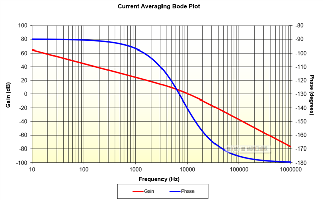
Hi
I am using UCC28019A for power facror correction.
How can I determine that the phase compensation design of this IC is OK?
Is it sufficient if the gain and phase margins in Figures 30 and 32 are satisfied independently?(Datasheet Figure 30,32)