- Ask a related questionWhat is a related question?A related question is a question created from another question. When the related question is created, it will be automatically linked to the original question.
This thread has been locked.
If you have a related question, please click the "Ask a related question" button in the top right corner. The newly created question will be automatically linked to this question.
Tool/software:
Dear TI Team,
I am currently working on a setup involving the AFE7950EVM, where I aim to generate a 1 GHz sine wave, send it to the DAC, and process the looped-back ADC data via the FPGA JESD interface. I have a few queries and would greatly appreciate your assistance in resolving them:
DAC Sampling Rate:
The DAC sampling rate displayed in the Latte GUI is mentioned as 2949.12 * 4 = 11,796.48 MSPS. Could you please explain why this multiplication by 4 is performed? and I can change or not how?
Frequency Calculation for Custom Sine Wave (64-point LUT):
I calculated the sine wave frequency as 184.32 MHz(clock) / 64(point) = 2.88 MHz based on the customized 64-point sine wave generated from the sine_64point.v Verilog code. Is this the correct frequency? If not, could you clarify the expected frequency? given 64 point Verilog code?
NCO Frequency Configuration:
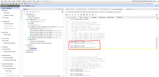
In the Latte GUI, I modified the NCO frequency using the following configuration:
Are there additional configurations I need to ensure proper operation, or is this sufficient?
SYSREF and Reference Clock:
I have connected sysref_p and sysref_n from the AFE7950EVM to the FPGA. The system clock (sys_clock) is set to 184.32 MHz, as specified by the EVM.
wire sysref;
IBUFDS sysref_ibuf (.I(sysref_p), .IB(sysref_n), .O(sysref));
assign rx_sysref = sysref;
assign tx_sysref = sysref;
Could you confirm the reference clock (ref clock) frequency from the AFE7950?
JESD Data Rate and Sampling Rates:
After processing through the JESD interface, what is the expected data rate? How is this data rate related to the ADC and DAC sampling rates?
1 GHz Sine Wave LUT:
Could you provide a LUT or samples data for generating a 1 GHz sine wave using the AFE7950 DAC?
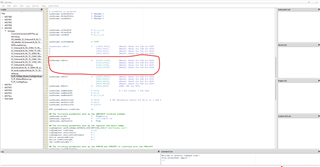
gui

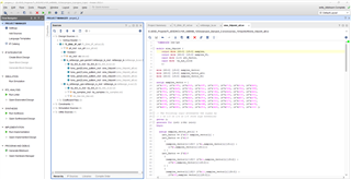
verilog code

I have connected the DAC output to the ADC input via RF cable (J9 to J3) on the AFE7950EVM. I look forward to your guidance to ensure proper configuration and understanding of the data flow.
Thank you.
Best regards,
Banoth Balu
Dear TI Support Team,
I am currently working with the AFE7950 DAC and have encountered some challenges related to the output signal when using a 12-point sine wave configuration.
I have attached a detailed document outlining my setup, observations, and specific questions about the DAC operation and configuration.
Attachment:
Request: I kindly request your review of the attached document and guidance on resolving the issue. Any insights or recommendations would be greatly appreciated.

I modified the NCO frequency to 1 GHz using the GUI and wrote a Python script to generate the 12-point sine wave.
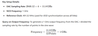
I wanted to confirm if this approach is correct for achieving a 1 GHz signal from the DAC ?.
'''
Validation :  AFE79xx Library Version
				v1.67, v1.74
Case			RX					TX						   FB						CLK					Notes
----	-----------------	  -----------------			-----------------			-----------			------------
1		245.76Msps, 24410     491.52Msps, 44210			491.52Msps, 22210			FADC=2949.12M       DAC in interleaved mode
		SerDes=9830.4Mbps     SerDes=9830.4Mbps			SerDes=9830.4Mbps			FDAC=8847.36M
		PLL0, NCO=3500M		  PLL0, NCO=3500M			NCO=3500M                   REF=491.52M

2		245.76Msps, 24410     491.52Msps, 44210			491.52Msps, 22210			FADC=2949.12M       DAC in straight mode
		SerDes=9830.4Mbps     SerDes=9830.4Mbps			SerDes=9830.4Mbps			FDAC=8847.36M
		PLL0, NCO=3500M		  PLL0, NCO=3500M			NCO=3500M                   REF=491.52M
'''
setupParams.skipFpga 				= 1
sysParams							= AFE.systemParams
setupParams.fpgaRefClk 				= 184.32
AFE.systemStatus.loadTrims			= 1

sysParams.fbEnable = [False]*2
sysParams.FRef                    	= 491.52
sysParams.FadcRx                  	= 2949.12     #adc sampling Rate
sysParams.FadcFb				  	= 2949.12
sysParams.Fdac                    	= 2949.12*4   #DAC sampling rate

sysParams.enableDacInterleavedMode	= False 					#DAC interleave mode to save power consumption. Fs/2 - Fin spur occurs

sysParams.modeTdd 					= 0
										# 0- Single TDD Pin for all Channels
										# 1- Separate Control for 2T/2R/1F
										# 2- Separate Control for 1T/1R/1F

sysParams.topLevelSystemMode		= 'StaticTDDMode'
sysParams.RRFMode 					= 0   #4T4R2F FDD mode
sysParams.jesdSystemMode			= [3,3]
										#SystemMode 0:	2R1F-FDD						; rx1-rx2-fb-fb
										#SystemMode 1:	1R1F-FDD						; rx1-rx1-fb-fb
										#SystemMode 2:	2R-FDD							; rx1-rx1-rx2-rx2
										#SystemMode 3:	1R								; rx1-rx1-rx1-rx1
										#SystemMode 4:	1F								; fb-fb-fb-fb
										#SystemMode 5:	1R1F-TDD						; rx1/fb-rx1/fb-rx1/fb-rx1/fb
										#SystemMode 8:	1R1F-TDD 1R-FDD	(FB-2Lanes)(RX1 RX2 interchanged)		; rx2/fb-rx2/fb-rx1-rx1


sysParams.jesdLoopbackEn			= 0 #Make it 1 to Enable the JESDTX to JESDRX internal loopback
sysParams.LMFSHdRx                	=['44210', '44210', '44210', '44210']
										# The 2nd and 4th are valid only for jesdSystemMode values in (2,6,7,8). For other modes, select 4 converter modes for 1st and 3rd.
sysParams.LMFSHdFb                	= ["22210","22210"]

sysParams.LMFSHdTx                	= ["44210","44210","44210","44210"]

sysParams.jesdTxProtocol            = [2,2]    #64b/66b
sysParams.jesdRxProtocol            = [2,2]    #64b/66b
sysParams.serdesFirmware			= True 		# If you want to lead any firmware, please speify the path here. Otherwise it will not write any firmware
sysParams.jesdTxLaneMux				= [0,1,2,3,4,5,6,7]
												# Enter which lanes you want in each location.
												# Note that across 2T Mux is not possible in 0.5.
												# For example, if you want to exchange the first two lines of each 2T, this should be [[1,0,2,3],[5,4,6,7]]
sysParams.jesdRxLaneMux				= [0,1,2,3,4,5,6,7]
												# Enter which lanes you want in each location.
												# Note that across 2R Mux is not possible in 0.5.
												# For example, if you want to exchange the first two lines of each 2R, this should be [[1,0,2,3],[5,4,6,7]]

sysParams.jesdRxRbd					= [4, 4]

# scrambler is disabled
sysParams.rxJesdTxScr				= [False]*4
sysParams.fbJesdTxScr				= [False]*2
sysParams.jesdRxScr					= [False]*4


sysParams.rxJesdTxK					= [1,1,1,1]
sysParams.fbJesdTxK					= [1,1]
sysParams.jesdRxK				    = [1,1,1,1]


sysParams.ncoFreqMode 				= "FCW"

#sysParams.txNco0					= 	[[9500,9500],		#Band0, Band1 for TxA for NCO0
#										[9500,9500],        #Band0, Band1 for TxB for NCO0
#										[9500,9500],        #Band0, Band1 for TxC for NCO0
#										[9500,9500]]        #Band0, Band1 for TxD for NCO0


sysParams.txNco0					= 	[[1000,1000],		#Band0, Band1 for TxA for NCO0
										[1000,1000],        #Band0, Band1 for TxB for NCO0
										[1000,1000],        #Band0, Band1 for TxC for NCO0
										[1000,1000]]        #Band0, Band1 for TxD for NCO0


#sysParams.rxNco0					= 	[[9500,9500],		#Band0, Band1 for RxA for NCO0
#										[9500,9500],        #Band0, Band1 for RxB for NCO0
#										[9500,9500],        #Band0, Band1 for RxC for NCO0
#										[9500,9500]]        #Band0, Band1 for RxD for NCO0


sysParams.rxNco0					= 	[[1000,1000],		#Band0, Band1 for RxA for NCO0
										[1000,1000],        #Band0, Band1 for RxB for NCO0
										[1000,1000],        #Band0, Band1 for RxC for NCO0
										[1000,1000]]        #Band0, Band1 for RxD for NCO0


sysParams.fbNco0					= 	[9500,9500]			#FBA, FBC for NCO0

sysParams.numBandsRx				= [0]*4					# 0 for single, 1 for dual
sysParams.numBandsFb				= [0,0]
sysParams.numBandsTx				= [0,0,0,0]

sysParams.ddcFactorRx             	= [4]*4			# DDC decimation factor for RX A, B, C and D
sysParams.ddcFactorFb             	= [4]*2
sysParams.ducFactorTx             	= [16]*4

AFE.systemStatus.loadTrims			=1

## The following parameters sets up the LMK04828 clocking schemes
lmkParams.pllEn						=	True#False
lmkParams.inputClk					=	1474.56#737.28
lmkParams.lmkFrefClk				=	True

## The following parameters sets up the register and macro dumps
logDumpInst.setFileName(ASTERIX_DIR+DEVICES_DIR+r"\Afe79xxPg1.txt")
logDumpInst.logFormat				= 0x0
logDumpInst.rewriteFile				= 1
logDumpInst.rewriteFileFormat4		= 1
device.optimizeWrites				= 0
device.rawWriteLogEn				= 1
lmk.rawWriteLogEn = 1

## The following parameters sets up the SYNCIN and SYNCOUT to interface with the TSW14J57
sysParams.jesdABLvdsSync			= 1
sysParams.jesdCDLvdsSync			= 1
sysParams.rxJesdTxSyncMux			= [0,0,0,0]
sysParams.fbJesdTxSyncMux			= [0,0]
sysParams.jesdRxSyncMux				= [0,0,0,0]		#[0,0,1,1]
sysParams.syncLoopBack				= True


# ## The following parameters sets up the AGC
# sysParams.agcParams[0].agcMode = 1 ##internal AGC
# sysParams.agcParams[0].gpioRstEnable = 0 ##disable GPIO based reset to AGC detector
# sysParams.agcParams[0].atken = [0, 1, 0] ##enable big and small step attack
# sysParams.agcParams[0].decayen = [0,1,0] ##enable big and small step decay
# sysParams.agcParams[0].atksize = [2,1,0] ## bigs step = 2dB, small step = 1dB
# sysParams.agcParams[0].decaysize = [2,1,0] ##big step = 2dB, small step = 1dB
# sysParams.agcParams[0].atkthreshold = [-1, -2, -14] ##attack threshold
# sysParams.agcParams[0].decaythreshold = [-14, -6, -20] ##decay threshold
# sysParams.agcParams[0].atkwinlength = [170, 170] ## detector time constant expressed inn absolute time in ns.
# sysParams.agcParams[0].decaywinlength = 87380 ##detector time constant expressed in absolute time in ns. All detectors use the same value for decay time constant
# sysParams.agcParams[0].atkNumHitsAbs = [8,8] ##absolute number of times signal crosses threshold. These crossing are with respect to the FADC/8 clock
# sysParams.agcParams[0].decayNumHitsAbs = [100,100] ##absolute number of times signal crosses threshold. These crossing are with respect to the FADC/8 clock
# sysParams.agcParams[0].minDsaAttn = 0 ##minimum DSA attenuation used by AGC
# sysParams.agcParams[0].maxDsaAttn = 22 ##maximum DSA attenuation used by AGC
# sysParams.agcParams[0].totalGainRange = 22 ##total gain range used by ALC for gain compensation
# sysParams.agcParams[0].minAttnAlc = 0 ##minimum attenuation used by ALC for compensation when useMinAttnAgc = 0
# sysParams.agcParams[0].useMinAttnAgc = 1 ##enable ALC to use minimum attenuation from AGC for which compensation is required.
# sysParams.agcParams[0].alcEn = 1
# sysParams.agcParams[0].alcMode = 0 ##floating point DGC
# sysParams.agcParams[0].fltPtMode = 0 ##if exponent > 0, dont send MSB
# sysParams.agcParams[0].fltPtFmt = 1 ##3 bit exponent


## The following parameters sets up the GPIOs
sysParams.gpioMapping={
		'H8': 'ADC_SYNC0',
		'H7': 'DAC_SYNC0',
		'N8': 'ADC_SYNC2',
		'N7': 'ADC_SYNC3',
		'H9': 'ADC_SYNC1',
		'G9': 'DAC_SYNC1',
		'N9': 'DAC_SYNC2',
		'P9': 'DAC_SYNC3',
		'P14': 'GLOBAL_PDN',
		'K14': 'FBABTDD',
		'R6': 'FBCDTDD',
		'H15': ['TXATDD','TXBTDD'],
		'V5': ['TXCTDD','TXDTDD'],
		'E7': ['RXATDD','RXBTDD'],
		'R15': ['RXCTDD','RXDTDD']}

#AFE.systemParams.papParams[0]['enable'] = True
#AFE.systemParams.papParams[1]['enable'] = True
#AFE.systemParams.papParams[2]['enable'] = True
#AFE.systemParams.papParams[3]['enable'] = True

device.delay_time = 0
## Initiates LMK04828 and AFE79xx Bring-up
setupParams.skipLmk	=	False
AFE.initializeConfig()
lmkParams.sysrefFreq = AFE.systemStatus.sysrefFreq
lmkParams.lmkPulseSysrefMode = False
AFE.LMK.lmkConfig()One more point: regarding lanes in gui 0 1 2 3 4 5 6 7
In .vh hedder file in verilog given for dac 4,5,6,7,3,0,1,2 and adc 5,4,6,7,3,0,1,2

Best regards,
balu