

Hi TI Experts,
Can you provide a List of collaterals that can be referred when starting a custom board hardware design?

Hi TI Experts,
Can you provide a List of collaterals that can be referred when starting a custom board hardware design?
Hi Board designers,
The below links are a quick reference to the collaterals that can be referred when starting a custom design.
Device Selection and features
Product Pages
https://www.ti.com/product/AM3351
https://www.ti.com/product/AM3352
https://www.ti.com/product/AM3354
https://www.ti.com/product/AM3356
https://www.ti.com/product/AM3357
https://www.ti.com/product/AM3358
https://www.ti.com/product/AM3359
Datasheet
AM335x Sitara Processors datasheet
https://www.ti.com/lit/pdf/sprs717
Updated Device Comparison
AM335x_Device Features Comaprison_Updated.xlsx
Silicon Errata
AM335x Sitara Processors Silicon Revisions 2.1, 2.0, 1.0
https://www.ti.com/lit/pdf/sprz360
Technical Reference Manual
AM335x and AMIC110 Sitara Processors Technical Reference Manual
https://www.ti.com/lit/pdf/spruh73
Custom Board design
Hardware Design Guide
AM335x Hardware Design Guide
https://www.ti.com/lit/pdf/sprabu5
Schematic Checklist
AM335x Schematic Checklist
https://www.ti.com/lit/pdf/sprabn2
Previous revision that includes RTC information
2.14 RTC
Table 2 describes what to do with each pin related to RTC functionality. Three use case scenarios are
provided:
• RTC-only mode: If you will be using the low power RTC-only mode. This use case allows low power
operation of the AM335x by allowing only the RTC power supply to be ON while all the remaining
supplies are OFF.
• RTC timer functionality but no RTC-only mode: If you will be using the RTC feature but do not need
RTC-only mode. This use case allows you to use the Real Time clocking features (keeping time), but
you do not need to support the low power RTC-only mode.
www.ti.com References
SPRABN2–March 2019 9
Submit Documentation Feedback
Copyright © 2019, Texas Instruments Incorporated
AM335x schematic checklist
• RTC feature disabled: If you will never use the RTC features. In this use case, the RTC functions are
fully disabled.
And for software configuration, follow https://www.ti.com/lit/pdf/sprack4
Evaluation – EVM
https://www.ti.com/tool/TMDSICE3359
BEAGL-BONE-GRN-ECO
Seeed Studio BeagleBone® Green eco evaluation module
https://www.ti.com/tool/BEAGL-BONE-GRN-ECO
BeagleBone_Green_REV1.1_SCH.pdf
The Below SK has been retired. For SK schematics refer the below E2E links
https://www.ti.com/tool/TMDSSK3358
(+) TMDSSK3358: Schematic design files - Processors forum - Processors - TI E2E support forums
(+) TMDSSK3358: Wrong board or wrong gen.? - Processors forum - Processors - TI E2E support forums
https://www.ti.com/tool/TMDXEVM3358
Evaluation – EVM LCD schematics
AM335X_EVM_LCDA_3H0005_SCHEMATIC_REV1_1A.pdf

6761.AM335X_EVM_LCDA_3H0005_SCHEMATIC_REV1_1A.pdf
AM335X_EVM_LCDA_3H0005_REV1_3A.pdf
AM335X_EVM_LCDA_3H0005_REV1_2A.pdf
Base board schematics PDF
5050.AM335X_gpevm_ZCZBASEBOARD_3H0002_REV1_4A.pdf
Daughter board schematics pdf
7183.AM335X_GPDAUGHTERBOARD_3H0001_SCHEMATIC_REV1_1A.pdf
There seems to be a muxed GPMC interface implemented.
https://media.digikey.com/pdf/Data%20Sheets/Texas%20Instruments%20PDFs/TMDXICE3359_SCH.pdf
2 x 8 bit DDR# interface
TMDXEVM3358 Evaluation board | TI.com
https://www.ti.com/lit/zip/sprr164
CAD symbols
CAD symbol specific to the selected device can be chosen from the device product page. Refer below example:
https://www.ti.com/product/AM3351#cad-cae-symbols
Ordering & quality
https://www.ti.com/product/AM3351#order-quality
https://www.ti.com/product/AM3352#order-quality
https://www.ti.com/product/AM3354#order-quality
https://www.ti.com/product/AM3356#order-quality
https://www.ti.com/product/AM3357#order-quality
https://www.ti.com/product/AM3358#order-quality
https://www.ti.com/product/AM3359#order-quality
Documents for ZCE, could be useful to the customer drawing PCB.
https://www.ti.com/lit/pdf/mpbgat2
https://www.ti.com/lit/pdf/mpbg896
DDR Board Design and Layout Guidelines
Datasheet reference
7 Peripheral Information and Timings
7.7.2 mDDR(LPDDR), DDR2, DDR3, DDR3L Memory Interface
Design Simulation files
https://www.ti.com/product/AM3359#design-tools-simulation
Simulation files provided includes
AM335x Thermal Model, BSDL models, IBIS models, CLOCKTREETOOL, Power Estimation Tool (PET),
IBIS, IBIS-AMI, BSDL, Thermal model and power-estimation tool (PET), SITARA-DDR-CONFIG-TOOL, PROCESSORS-3P-SEARCH
Technical Documents
Collaterals and application notes
https://www.ti.com/product/AM3359#tech-docs
Technical Support
AM3351, AM3352, AM3354, AM3356, AM3357, AM3358, AM3359 Custom board design - FAQs
Previous E2E threads - Keywords AM335x, AM3351, AM3352, AM3354, AM3356, AM3357, AM3358, AM3359
Starting a new thread
Notes
Regards,
Sreenivasa

Hi Board designers,
Refer below:
AM3352: Update on Sitara Device/Family longevity and roadmap processor family
there is currently no plans to End of Life AM335x for the foreseeable future. Please feel free to continue to use it, however if you would like to check out our current generation arm processors, i recommend AM62x or AM62L.
Regards,
Sreenivasa
Hi Board designers,
Inputs regarding Package shelf life
Please refer below links
https://www.ti.com/support-quality/quality-policies-procedures/product-shelf-life.html
https://www.ti.com/support-quality/faqs/product-shelf-life-faqs.html
https://www.ti.com/support-quality/reliability/reliability-home.html
https://www.ti.com/lit/an/spraby1a/spraby1a.pdf
https://www.ti.com/lit/pdf/snoa550
https://www.ti.com/lit/an/slva840/slva840.pdf
/cfs-file/__key/communityserver-discussions-components-files/791/Baking-Procedure.pdf
I got the ask from a customer if we define the storage air humidity and the air humidity in operation for the AM62P?
I guess not, but I wanted to doublechekc with you.
Also, this is the requirements they are asking for:
Prior to board assembly but removed from sealed packaging -> device is specified as MSL3, rated for 168hrs exposure at ≤30°C/60%RH ambient conditions without a re-bake being required before board assembly.
We have no spec for operational humidity specification, but device completed and passed relevant qualification at MSL3 moisture precondition + 1000hrs 85°C/85%RH THB (Temperature, Humidity, Bias) per standard JEDEC test conditions
Regards,
Sreenivasa
Hi Board Designers,
Refer additional inputs:
following signal pins and power domains are not used in the design of my customer, how this pins should be connected (pulled up, down or unconnected)?
- VDDA1P8V_USB0
- VDDA1P8V_USB1
- VDDA3P3V_USB1
- USB0_CE (not used because USB0 is used as device)
- USB0_ID (not used because USB0 is used as device)
- USB0_DRVVBUS (not used because USB0 is used as device)
- USB1DP
- USB1DM
- USB1_VBUS
- USB0_DRVVBUS
- USB1_DRVVBUS
- USB1DP
- USB1DM
- USB1_VBUS
- USB1_DRVVBUS
- VDDA_ADC
- AIN0 - AIN7
- VREFN/VREFP
- EXTINT (RTC-MODE)
- EXT_WAKEUP (RTC-MODE)
Some of your questions could be answered by reviewing the AM335x Data Sheet (http://www.ti.com/product/am3358) and AM335x Schematic Checklist (http://processors.wiki.ti.com/index.php/AM335x_Schematic_Checklist).
Why do you say VDDA1P8V_USB0 is not being used when you also say USB0 is used as device? This is power supply is required if you are using USB0.
The schematic check list and a note attached to each power sequence waveform shown in Section 4.1 of the data sheet describes how the respective VDDA1P8V_USBx and VDDA3P3V_USBx should be connected when not using one of the USB ports.
I do not understand your comment “not used because USB0 is used as device” attached to the USB0_CE pin. This is an optional output that can be used to enable a battery charger when the product is a battery powered device that allows the battery to be charged from a USB host or dedicated charger. It does not need to be connected if not using the charger detect circuit in the USB PHY to enable an external battery charger.
I think the USB data pins can be left unconnected when the USB port is not used, but I need to verify.
USBx_DRVVBUS can be left unconnected or configured as a GPIO if the respective USB port is not configured to operate in USB host mode.
The schematic check list describes how the VDDA_ADC should be connected when not using the ADC.
I assume the ADC inputs and reference voltage inputs should also be connected to ground when not using the ADC, but I need to verify.
I do not understand your comment “RTC-mode” attached to the EXTINTn pin. The EXTINTn input doesn’t have anything to do with the RTC. This is an external interrupt to the ARM-A8 processor. As described in the AM335x Silicon Errata (Advisory 1.0.6) this input was accidently inverted such that it is active high with an internal pull-up on the current version of silicon. However, this will be changed on the next version of silicon. This input will be changed to be active low with an internal pull-up. Customers need to account for this change now while designing their PCB if they are using this input.
EXT_WAKEUP is an active high input used to wakeup the system from deep sleep when the device power is controlled the RTC. This version of silicon has a problem supporting RTC based deep sleep which is described in the AM335x Silicon Errata (Advisory 1.0.5). The customer may want to use this input on the next version of silicon when this problem has been fixed. If so, they could connect external wakeup events to this input to request the RTC to enable the power source.
Should customer power both rails VDDA1P8V_USB0 and VDDA3P3V_USB0, if they use 3,3V output?
Sorry, I just forwarded direct request from the customer without filtering it properly, sure EXTINTn has nothing to do with RTC...
So should they just leave these two pins (EXTINTn and EXT_WAKEUP) unconnected?
I do not understand the first question in your previous reply. If a USB port is used, both 1.8 volt and 3.3 volt power supply pins of the respective port must be sourced with the recommended voltage. What made you or the customer think the 3.3 volt supply may not be required when using the USB port?
VBUS and ID pins can be grounded or left floating.
CE should be left floating.
DP and DM pins can be grounded or left floating.
The VDDA1P8V pin must be sourced with the recommended voltage and would prefer to have the VDDA3P3V pin sourced with the recommended voltage. However, the VDDA3P3V pin can be connected to ground if the system doesn’t have a 3.3 volt supply.
The otg_pwrdn and cm_pwrdn bits in the respective USB_CTRL register can be used to power down the USB PHY if not using the USB port. These bits default to the powered-up state after device reset. The power supply leakage for the USB PHY can be minimized by setting both of these bits low when not using the USB port.
I am still checking on the ADC pins.
The answer to your last question depends if they plan to use the RTC enabled deep sleep feature with the next silicon revision and if they plan to connect any external interrupt sources. If the answer to both is no, then they do not need to connect these pins. However, I would connect the EXTINTn pin to an external pull-up resistor and the EXT_WAKEUP pin to an external pull-down resistor if it were my board design. This would provide an easy connection point on the board in case there were a future need to connect something to these inputs.
I have confirmed the VREFP and VREFN reference voltage inputs, AIN[7:0] analog inputs, and VDDA_ADC power supply input should be connected to ground when not using the ADC.
Regards,
Sreenivasa
Hi Board Designers,
The below FAQ includes E2E links that can be referenced during custom board design
Regards,
Sreenivasa
Hi Board designers,
Inputs regarding weight and material content

https://www.ti.com/materialcontent/home
Regards,
Sreenivasa
Hi Board Designers.
Inputs related to DDR3 VTT terminations:
Hello Experts,
I have a customer using DDR3 x16 single device.
In the data sheet we do not have differential clock termination when x1 device is used and no VTT termination Is used.
For the DDR4 we are recommending clock termination even when VTT termination for address and control signals are not used.
Any thoughts if the differential clock termination is recommended for DDR3 when VYY termination is not used and X1 16-bit memory is used.
With proper trace impedance, we have never required that the differential clock be terminated for single device DDR3 designs with AM335x. Don’t forget, AM335x max DDR freq is 400MHz (vs 800MHz for AM64x), so I believe we started recommending this for AM64x and beyond due to the increased frequencies. I found some discussion of this here: https://e2e.ti.com/support/processors-group/processors/f/processors-forum/215147/am335x-ddr3-ck-and-addr_ctrl-routing-why-source-termination-series-resistor-at-driver-is-not-allowed-under-a-single-chip-16bits-ddr3-case
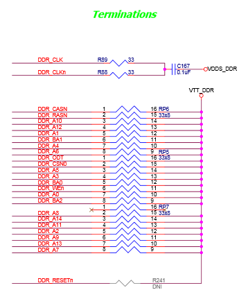
AM5746: DDR3 VTT Termination in IDK Schematic
Regarding the following marked area of TMDSIDK574 Schematic Sheet 10,
my customer has the following questions.

-Q1. Purpose and application of capacitors
-Number of capacitors required
Q2: Is it correct to assume that the required quantity differs for each artwork?
Q3: What is the recommended number of capacitors for the initial design?
-Condenser placement when designing artwork
Q4: Where is the optimal mounting position? Please let us know the mounting position.
Q5: When describing a capacitor in a circuit diagram,
should it be placed near the termination section, as shown in the circuit diagram above?
The VTT regulator can both source and sink current. The purpose of the VTT termination decoupling capacitors is to minimize the amount of noise on termination supply (VTT) by providing optimum path for return currents. Yes - the specific number of capacitors may vary with different design, the EVM reference is a good starting point. The DDR3 signals are routed in daisy-chain fashion - source to load to load to termination resistor. Typically a VTT plane segment is created for the termination resistors, and the plane segment has several decoupling capacitors to service all signals.
AM3358: Matching DDR3 Clock Trace Length between classes
AM3359 Processor SoC is having a DDR3L interface(2 nos of 4Gb x8 DDR3 chips MT41K512M8) in our board. We are planning to run at max speed of 400MHz DDR3 clock and max addressing of 1GB as per the datasheet. Board is in the final layout review stage and fly by termination topology is followed. Clock/Address/Command signals are routed first to 2nd DDR3 SDRAM (DDR chip with DQ8 to DQ15) and then next to 1st DDR3 SDRAM(DQ0 to DQ7) before getting terminated as shown in the block diagram. Is it fine to route the clock/address/command signals in this order ? Please let me know.

Yes, this should be ok. Be sure that you followed the layout guidelines in the datasheet. And for software configuration, follow https://www.ti.com/lit/pdf/sprack4
Figure 7-48 shows 16-Bit DDR3 interface using one 16-bit DDR3 device without Vtt termination. Neither termination resistors nor regulator are used in this case. However take note of section 7.7.2.3.3.9 comments:
"Figure 7-48 provides an example DDR3 schematic with a single 16-bit DDR3 memory device that does not have VTT termination on the address and control signals. A typical DDR3 point-to-point topology may provide acceptable signal integrity without VTT termination. System performance should be verified by performing signal integrity analysis using specific PCB design details before implementing this topology."
AM4372: DDR3 VTT termination resistor value
I have a question about the schematics of AM437x EVM.
May I use the same VTT termination resistor value on DDR_CLKx and other lines?
TRM specifies Zo as 50 ohm +/- 5ohm.
But I am curious why SK/EVM is put different resistor value.(DDR_CLKx are 49.9ohm, others are 47ohm)
Our target board is instable to read/write to/from DDR3.
I would like to clarify if we should follow EVM schematic. (47ohm and 49.9ohm)
Or, should follow TRM?.(50ohm +/-5ohm)
Best regards, RY


AM5728: EVM DDR3 circuit design confirmation
We can see capacitor between VTT and VDD_DDR at below fig, and VDD_DDR has bypass capacitor. What's the function at below capacitor

The purpose it to provide decoupling to the termination rail as well as minimize noise between the termination rail and the IO rail.
AM335x DDR3 VTT termination with Bypass Capacitors
With regards to AM3352's VTT termination on the address and control signals,
below E2E post mentions the address/control signals should have far-end parallel terminated to a VTT supply.
e2e.ti.com/.../160622
But as per the AM335x StarteKit's schematics, these lines seems to be just pulled-up to the VTT_DDR.
Can we assume the proper way of parallel termination is to pull-up the address and control signals
to VTT supply similar to the starterkit?
Yes, on the Starter Kit schematic the VTT supply is shown just below the termination resistors. Please not that value of 50Ohms should be used for the termination resistors, not 33Ohms. See parameters 11 and 12 in Table 7-60 from the AM335X Datasheet Rev. H. The recommended value for Zo is 50Ohms.
I generally discourage using VTT at all with AM335x. If you're using a 16-bit DDR3 device (i.e. point to point connection) it's really not needed. The BeagleBone Black is perhaps a better example with regard to DDR3 layout in this regard. You introduce a lot of additional complexity into the layout by terminating all the address/control lines, and this is frequently a place where mistakes are made. It also adds complexity in terms of controlling the "enable" pin of the VTT regulator (e.g. TPS51200) during suspend/resume which is another source of frequent issues.
Could you provide below specification for DDR3?
Clock to ADD/DQS/Data Output Skew) / Input Setup/Hold time
This should be defined in the DDR3 JEDEC spec. The interface is compatible with DDR3 devices that are JEDEC compliant to JESD79-3C
Regards,
Sreenivasa