This thread has been locked.

If you have a related question, please click the "Ask a related question" button in the top right corner. The newly created question will be automatically linked to this question.

[FAQ] AM6442, AM6441, AM6422, AM6421, AM6412, AM6411 and AM2434, AM2432, AM2431 (ALV, ALX) Custom board hardware design – Queries regarding Crystal selection and clock specifications

Part Number: AM6442
Other Parts Discussed in Thread: TMDS64EVM, , LMK1C1104, AM3352, AM62A3-Q1, AM62L, OMAP-L138, AM62A7

Hi TI Experts,

I have the below queries regarding the crystal selection.

  1. Recommended crystal frequency for MCU_OSC0
  2. Do you have recommended part numbers for Crystal? 
  3. Can you help check if NX2016SA-25MHZ-EXS00A-CS10694, CRYSTAL 25.0000MHZ 8PF SMD could be used?
  4. Do you have recommendations for MCU_OSC0 crystal selection.
  5. Could you share the crystal part number used on the EVM? 
  6. Can i use an oscillator as the clock source?
  7. Is there a real max value for crystal ESR?
  8. Is there some guidelines for the crystal circuit layout?
  9. Is there a delay requirement for the MCU_PORz after all the power supplies ramp and does the delay depend on the clock source

Let me know your thoughts.

  • Hi Board designers, 

    Refer below inputs for the queries related to the MCU_OSC0 crystal selection. 

    1.Recommended crystal frequency for MCU_OSC0

    Recommended Crystal Parallel Resonance Frequency for MCU_OSC0 is 25 MHz

    2. Do you have recommended part numbers for Crystal? 

    "Note that we do not provide part number recommendations."

    The system requirements of a customer’s product need to be considered when selecting a crystal.  We do not know the operating conditions or frequency tolerance of all attached devices within their system.  The crystal requirements defined in our datasheet only address the processor requirements, but the crystal characteristics may also influence clocks that are sourced to attached devices which have their own requirements. In some cases, the attached devices may have frequency requirements that are tighter than the processor frequency requirements.

    3. Can you help check below specs and confirm this crystal specifications meets the requirements for the MCU_OSC0 Internal Oscillator Clock Source.

    The device expert and oscillator designer reviewed the crystal requirements and agree this crystal specifications meets the requirements for the HF oscillator implemented on our AM64x, AM62x and AM62Ax Sitara processors.

    4. Do you have recommendations for MCU_OSC0 crystal selection.

    Refer below sections of the device specific datasheet.

    AM64x SitaraTm Processors datasheet (Rev. E) (ti.com)

    Figure 7-17. MCU_OSC0 Crystal Implementation

    The crystal must be in the fundamental mode of operation and parallel resonant.

    Table 7-17. MCU_OSC0 Crystal Circuit Requirements summarizes the required electrical constraints.

    5. Could you share the crystal part number used on the EVM?

    TMDS64EVM

    ABM10W-25.0000MHZ-8-K1Z-T3

    25 MHz ±10ppm Crystal 8pF 50 Ohms 4-SMD, No Lead

    - Footprint = 100X80 mils (2.5 x 2.0mm)
    - CL = 8pF
    - ESRmax = 50
    - CSHUNTmax = 2pF
    - Temp grade = -40C~125C
    - CPCB = 12pF

    Do consider parasitic capacitance introduced by the PCB when determining the crystal load cap value.

    Alternate crystal parts that can be considered:


    Abracon ABM11W as alternate in 2.00mm x 1.60mm footprint...

    Digikey search results:

    https://www.digikey.com/en/products/filter/crystals/171?s=N4IgjCBcoCwGxVAYygMwIYBsDOBTANCAPZQDaIAHAKwUBMIAuoQA4AuUIAyqwE4CWAOwDmIAL6EwATgqTEIFJAw4CxMiAAMjcSFrq6chUryESkclXUACAPIALALbZGLdpBABVAX1bXUAWVx0bABXHlwxQlowCwM0LGNVMx0qSz8ACQAvZxA2Dk9vXwCg0PDRbXok9AAjHnQkIgEtIA


    ABM11W = Plated at exceptionally low plating capacitance, as low as 4pF, with optimized ESR


    ABM11W-25.0000MHZ-6-K1Z-T3

                    - Footprint = 80X60 mils (2.0x1.6mm)

                    - CL = 6pF

                    - ESRmax = 50ohms

                    - CSHUNTmax = 2pF

                    - Temp grade = -40C~125C

                    - CPCB(prelim) = 9pF


    ABM11W-25.0000MHZ-8-D1X-T3

                    - Footprint = 80X60 mils (2.0x1.6mm)

                    - CL = 8pF

                    - ESRmax = 50ohms

                    - CSHUNTmax = 2pF

                    - Temp grade = -40C~85C

                    - CPCB(prelim) = 13pF

    6. Can I use an oscillator as the clock source?

    Refer 7.10.4.1.2 MCU_OSC0 LVCMOS Digital Clock Source of the device-specific data sheet. Follow the recommended XO termination.

    7. Is there a real max value for crystal ESR?

    The maximum ESR recommended is 50 ohms regardless of shunt capacitance.

    8. Is there some guidelines for the crystal circuit layout?

    Refer 9.3 Clock Routing Guidelines, 9.3.1 Oscillator Routing section of the device-specific data sheet.

    9. Is there a delay requirement for the MCU_PORz after all the power supplies ramp and does the delay depend on the clock source?

    Refer to MCU_PORz Timing Requirements in the device-specific data sheet

    RST1 Hold time, MCU_PORz active (low) at Power-up after supplies valid (using external crystal circuit) is 9500000 ns
    RST2 Hold time, MCU_PORz active (low) at Power-up after supplies valid and external clock stable (using external LVCMOS clock source) 1200 ns (This does not include the external oscillator start-up time)

    Regards,

    Lavanya M R.

  • Hi TI Experts,

    I have the below additional queries regarding the crystal selection.

    10. MCU_OSC0_XI/MCU_OSC0_OUT starts before VDD_CORE voltage ramps up, is this a concern
    11. Does it have any side effect when MCU_OSC0_XI clock starts before VDD_CORE voltage ramps up? What kind of conditions let MCU_OSC0_XI doesn't start until after VDD_CORE is applied?
    12. It is assumed that when a crystal connected externally has a large change in frequency due to some factor, there will be an effect on the PLL.
    13. Does the 25MHz XTAL has an oscillation margin switching function and is there need to configure registers.
    14. Do you have some recommendations on the crystal load and load capacitance matching 

    Let me know your thoughts.

  • Hi Board designers, 

    Refer below inputs for the queries related to the MCU_OSC0 crystal selection. 

    10. MCU_OSC0_XI/MCU_OSC0_OUT starts before VDD_CORE voltage ramps up, is this a concern

    The oscillator is working as expected. It most cases the oscillation will start shortly after its 1.8V power rail is applied, but there may be conditions where it doesn't start until after VDD_CORE is applied.

    11. Does it have any side effect when MCU_OSC0_XI clock starts before VDD_CORE voltage ramps up? What kind of conditions let MCU_OSC0_XI doesn't start until after VDD_CORE is applied?

    No side effects.

    The oscillator has registers in the VDD_CORE power domain that controls some of its operating functions. It is very unlikely the start-up will be delayed until VDD_CORE is valid, but we are being conservative by saying the oscillation will not begin until VDD_CORE is valid to ensure the product designer provides adequate time for the oscillator to start before reset is released.

    (+) [FAQ] AM6442: question about MCU_OSC0 Start-up - Processors forum - Processors - TI E2E support forums

    [FAQ] AM6442: question about MCU_OSC0 Start-up

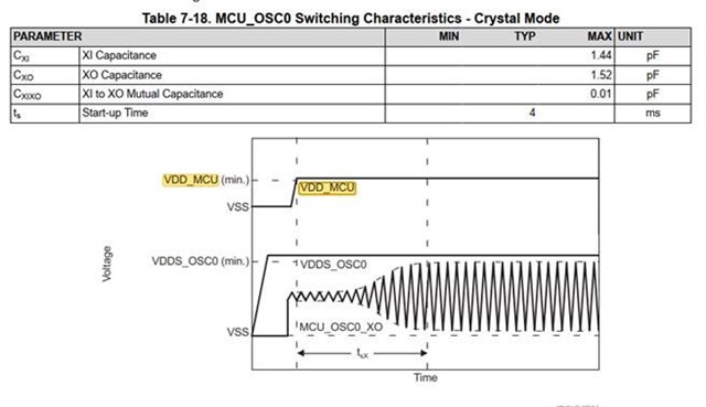
    I have a question about "Figure 7-16. MCU_OSC0 Start-up Time" from the datasheet. Here it looks like that MCU_OSC0 is only allowed to start when VDD_MCU is ramping. In reality the osciallation starts already with VDDS_OSC0, while VDD_MCU is still disabled. 

    I assume that this is OK and not causing any problems?! But if this is the case, why is the Start-up Time ts shown relatative to VDD_MCU stable? Shouldn't it be related to VDDS_OSC0 stable?


    The oscillator is powered from VDDS_OSC0. So it may power-up and begin oscillation as soon as VDDS_OSC0 is applied. However, the oscillator has a few control registers which are powered by the VDD_CORE domain. So there is a chance the oscillator may not start until the VDD_CORE is valid. 

    The supply shown in the upper waveform should be named VDD_CORE rather than VDD_MCU. AM64x does not even have a power rail named VDD_MCU. Therefore, I need to get this figure updated in the datasheet. Thanks for asking the question, which highlighted the error in the figure. 


    12. It is assumed that when a crystal connected externally has a large change in frequency due to some factor, there will be an effect on the PLL.

    I would like to know the effect on the PLL when the frequency changes and how each function will operate. The factors that may cause the frequency to change include initial failure, environment, and manufacturing defects.

    Ans: It is not possible for crystals to have a large change in frequency. They have a very high-Q impedance response. The impedance drops dramatically with a very small shift in frequency, which would cause the gain in the oscillator feedback path to drop such that it is not possible to maintain oscillation. So, they are either oscillating at their designed frequency are not oscillating.

    13. Does the 25MHz XTAL has an oscillation margin switching function and is there need to configure registers.

    No HFOSC0 registers are required to be changed. These registers should remain in their default state.
    Select the appropriate crystal circuit components that are compliant to the values defined in the MCU_OSC0 Crystal Circuit Requirements table.
    Read the Load Capacitance and Shunt Capacitance sections to select the appropriate crystal circuit components.

    14. Do you have some recommendations on the crystal load and load capacitance matching 

    It is recommended to match the crystal load and the load capacitance as per the data sheet recommendations. Any difference in the crystal load and the load cap capacitance selected could result in PPM variation of the clock frequency Choose crystal load as per the standard capacitance availability to ensure matching of the capacitance.

    References

    https://e2e.ti.com/support/processors-group/processors/f/processors-forum/1115457/am6411-is-it-needed-to-input-the-synchronized-clock-between-am64x-and-ethernet-phy

    Regards,

    Sreenivasa

  • Hi Board designers, 

    Additional references:

    MCU_OSC0 LVCMOS Digital Clock Source

    https://e2e.ti.com/support/processors-group/processors/f/processors-forum/1381636/am6442-for-pin-c21-b20-we-use-lvcoms-digital-osc-how-should-i-connect-c21-and-b20-i-didn-t-found-the-specification-thanks/5279659

    (+) AM6412: AM64x MCU_OSC0 LVCMOS Digital Clock Source specification - Processors forum - Processors - TI E2E support forums

    (+) [FAQ] AM6442, AM6441, AM6422, AM6421, AM6412, AM6411 and AM2434, AM2432, AM2431 (ALV, ALX) Custom board hardware design – Queries regarding MCU_OSC0 LVCMOS Digital Clock Source - Processors forum - Processors - TI E2E support forums

    Connection of LVCMOS clock input

    1.8V LVCMOS-Compatible Clock Input

    The clock inputs are not fail-safe

    The clock inputs are referenced to 1.8V, VDDS_OSC0.

    The Clock input is not fail-safe

    It is recommended to connect the Oscillator supply to the same supply that is connected to the VDDS_OSC0

    Is there any concerns using LVCMOS clock input

    Using a crystal to create a reference clock for AM62x family of processors is preferred because there is less risk of clock jitter issues.

    There is no concern using LVCMOS clock input. Follow the above specifications while selecting the oscillator. If you use a LVCMOS oscillator, select one that doesn't contain a PLL. LVCMOS clock sources that only implement a crystal oscillator operating in fundamental oscillation mode provides lower clock jitter than one with a PLL.

    Ensure you follow the Note added in the MCU_OSC0 LVCMOS Digital Clock Source section of the data sheet 

    (8) [FAQ] AM2434: A DC steady-state condition is not allowed on MCU_OSC0_XI - Arm-based microcontrollers forum - Arm-based microcontrollers - TI E2E support forums

    There is the description “A DC steady-state condition is not allowed on MCU_OSC0_XI when the oscillator is powered up.” at 6.10.4.1.2 MCU_OSC0 LVCMOS Digital Clock Source in the datasheet.


    Why is inversion logic necessary?

    The inverter shown in the diagram was meant to represent an LVCMOS output, where the LVCMOS output could be the oscillator output buffer, or the LVCMOS output from some clock distribution device. There is no requirement to invert the clock source.

    Is it no problem that LMK1C1104 and LMK6CE02500 are directly connected to MCU_OSC0_XI like below ? or Should C-cut (C coupling) be needed ?

    You should connect the 1.8V LVCMOS clock source output directly to the XI pin and connect the XO pin to VSS.

    There are internal AC coupling capacitors in both of the XI and XO signal paths that connect to an internal comparator that creates a square wave from the crystal circuit oscillation. A DC steady-state condition on the XI pin relative to the XO pin would allow the comparator to generate glitches on the internal clock tree of the device and cause it to do unpredictable things.

    Regards,

    Sreenivasa

  • Hi Board designers, 

    Additional references for crystal selection

    https://e2e.ti.com/support/processors-group/processors/f/processors-forum/1038770/am3358-frequency-tolerance-and-frequency-stability-of-24mhz-crystal/3841749

    The accuracy of the AM335x reference clock source should be based on system level requirements. For example, you may need a 30 PPM reference clock if an AM335x timer is being used to operate something that needs this level of accuracy. 

    The 50 PPM limit was defined for AM335x because the RMII Ethernet standard requires this accuracy. The other Ethernet standards only require 100 PPM, so you may be able to back-off on this 50 PPM requirement if not using RMII. However, this depends if you have other system function that require an accuracy of 50 PPM. I would not recommend going above 100 PPM as this may begin to effect other peripheral interfaces.

    Keep in mind, a crystal has three contributions to accuracy. There is a parameter that defines initial accuracy, another parameter that defines accuracy over operating temperature, and aging parameter that defines how much the resonate frequency changes over time due to aging effects. When selecting a crystal, you must combine all of these to determine frequency accuracy across all operating conditions for the life of the product.

    Reliable start-up is also a concern with crystal selection. The max ESR of the crystal is one of the primary concerns. The AM335x oscillator may not have enough gain to reliably start oscillation if the crystal ESR is too low. Many crystal datasheets define a worst case max ESR value for the entire family of crystals rather than a specific max ESR for the crystal being selected. In most cases the higher frequency crystals in the family will have a much lower max ESR value that what is found in the datasheet. Therefore, you may need to contact the crystal manufacture and request a device specific datasheet for the crystal part number you plan to use.

    One way to confirm you have start-up margin, is by inserting a resistor in series with the selected crystal and checking for reliable start-up across all operating conditions. I suggest you begin with a resistor value that is about 5x the max ESR of the crystal. If you have start-up issues with this value you can reduce it to 3x. There is not enough gain margin if oscillation will not reliably start with a 3x resistor. You would need to select a crystal with lower ESR if you find it will not reliably start with a 3X series resistor.

    You neve said if you were using RMII and needed 50 PPM system performance. Therefore, I cannot comment how were these options align with your system requirements.

    I noticed the Digi-key description for your existing crystal, which they are selling under part number 7A-24.000MAAJ-T was cut for an 18pF load, so it must not be one of the standard options shown in the datasheet. What load did you apply to this crystal in your product? Are you willing to change load capacitor values in your product when you change crystals? How much capacitive load does you signals apply to the crystal circuit?

    I do not think a crystal cut for 18pF load was ever appropriate for AM335x. Each load capacitor would need to be approximately 33 - 36 pF to achieve a 18pF load for the crystal and the AM335x datasheet only allows load capacitors in the range of 12 - 24 pF. 

    The highest load capacitance crystal you would be able to use is 12pF to remain in the ranged defined by the AM335x datasheet.

    The AA-24.000MAHJ-T datasheet shows their standard offering is a crystal cut for a 8pF load. However, they provide an option to specify a load capacitance. I did not see an aging parameter in this datasheet, so not sure how PPM will change over time on this crystal.  It may be a viable option as long as you apply the correct load capacitance for the crystal your purchase while remaining compliant with AM335x datasheet. However, you should validate startup reliability using the method described previously to ensure ESR in not going to be a problem.

    The ECS-240-18-30-JGN-TR datasheet does not clearly show an option for buying a crystal cut for a lower capacitive load and 20 pF is too high. You may be able to use this as a viable option if they would sell you one that was cut for 10 pF.

    AM3352: Crystal OSC0 - Parameters - ESR and Behaviors

    https://e2e.ti.com/support/processors-group/processors/f/processors-forum/998892/am3352-crystal-osc0---parameters---esr-and-behaviors/3690471

    The biggest concern is not having enough gain margin to reliably start oscillation when the higher ESR crystal is combined with the other crystal circuit components and internal oscillator.

    There is a good chance you have enough gain margin if this combination of components has been used for a while without receiving any reports of the oscillator not starting.

    In most cases the actual ESR of a crystal is much smaller than the published value. This is especially true when the ESR value you are using is taken from a data sheet that covers an entire family of crystals. The max ESR value published in a crystal family data sheet is typically inflated to cover the entire range of crystals. You may be able to reach out to the crystal manufacture and request a part number specific datasheet to confirm the max ESR of your crystal.

    You can test the gain margin by placing a resistor in series with the crystal, which increases the ESR seen my the entire circuit. We typically recommend confirming reliable start of oscillation across operating conditions when the series resistor inserted increases the ESR to at least 3x the expected ESR of the crystal. 

    Load capacitor values should be selected based on the load expected by the crystal. Crystal are cut to oscillate at the specified frequency with a specific capacitive load. The frequency of oscillation will be pulled a few PPM from the specified frequency if the load you apply is not correct. Most crystal manufactures provide a service where they evaluate your product with their crystal and make recommendations if your initial component selection is not optimum. I think the fee they charge is reasonable for any high volume product where you want to be confident that you clock solution is robust.

    Regards,

    Sreenivasa

  • Hi Board designers, 

    Refer below FAQ for information related to Oscillator specifications being added to all the processor family data sheets and use of BAQ oscillator:

    (+) CDC6C: BAW oscillator use for AM6442 - Clock & timing forum - Clock & timing - TI E2E support forums

    LMK6CE02500DDLFT

    e2e.ti.com/.../am6442-can-i-use-this-oscillator

    Regards,

    Sreenivasa

  • Hi Board designers, 

    AM62A3-Q1: HW : crystal failure


    It is assumed that when a crystal connected externally has a large change in frequency due to some factor, there will be an effect on the PLL.

    I would like to know the effect on the PLL when the frequency changes and how each function will operate.

    The factors that may cause the frequency to change include initial failure, environment, and manufacturing defects.

    It is not possible for crystals to have a large change in frequency. They have a very high-Q impedance response. The impedance drops dramatically with a very small shift in frequency, which would cause the gain in the oscillator feedback path to drop such that it is not possible to maintain oscillation. So, they are either oscillating at their designed frequency are not oscillating.

    Regards,

    Sreenivasa

  • Hi Board designers, 

    Information related to clock source (oscillator) placed on carrier board:

    Q. The oscillator is placed on the carrier board and the clock is connected through a connector to the processor.
    My question was on the clock length and related concerns.
    Checking if there are any concern or care-abouts for customer to take care while placing the oscillator on the carrier board or should customer place the oscillator on the processor board and is there a recommendation or requirement to place oscillator close to processor like the crystal.

    A.

    The digital output of the LVCMOS clock source with fast rise/fall times will be more tolerant to noise than the near sinusoid signal that is produced by the crystal circuit, so placing it near the processor is not as important as the crystal circuit. They need to follow the recommendations in the following notes and confirm the Rise/Fall Time (10%-90% rise, 90%-10% fall) is less than 4ns at the MCU_OSC0_XI pin.
    Note
    1. A DC steady-state condition is not allowed on MCU_OSC0_XI when the oscillator is powered up. This is not allowed because MCU_OSC0_XI is internally AC coupled to a comparator that can enter an unknown state when DC is applied to the input. Therefore, application software must power down MCU_OSC0 any time MCU_OSC0_XI is not toggling between logic states. 2. The LVCMOS clock signal sourcing the MCU_OSC0_XI input must have monotonic transitions.
    The clock source should be connected to MCU_OSC0_XI with a point-to-point connection, via a series termination resistor placed near the clock source. The series termination resistor value should match the clock source output impedance to the transmission line impedance. For example, the series termination resistor value needs to be 20 ohms if the clock source has an output impedance of 30 ohms and the PCB signal trace has a characteristic impedance of 50 ohms. This allows the reflection that returns from the far end of the un-terminated transmission line to be completely absorbed such that is does not introduce any non-monotonic events on the signal.
    3. The PCB trace length connecting the LVCMOS clock source to MCU_OSC0_XI should be minimized. This reduces capacitive loading and decreases probability of external noise sources coupling into the clock signal. Reduced capacitive loading improves rise/fall times of the clock signal which reduces the probability of jitter being introduced in the system.

    My biggest concern is related to ground noise introduced by the two PCB implementation. Any ground noise (high frequency potential difference between the grounds of each PCB) will appears as noise on any signal that is sourced from a device on the carrier PCB to our device on the processor PCB. They need to have a lot of ground pins on the connectors that connect the two PCBs. I would say at least one ground for every two or three signals that transition from one board to the other.

    Regards,

    Sreenivasa

  • Hi Board designers, 

    Queries related to SOC start-up with crystal not operating

    Will it switch to CLK_12M_RC even if HFOSC0 is not oscillating at cold start?
    [TI] >> By default MCU_PLL_CLKSEL_CLKLOSS_SWTCH_EN is set to ‘0’. So at cold start, if HFOSC0 is not switching then the mux will not switch to CLK_12M_RC. If HFOSC0 is not switching during cold start, the device will not boot-up.

    Did you have a chance to power cycle the board and see the behavior with the oscillator disabled.

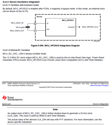
    5.4.4 Device Oscillators
    The device has the possibility to source clocks of an external high-frequency oscillator - MCU_HFOSC0. The
    device has also one internal RC oscillator - MCU_RC_OSC_12M.

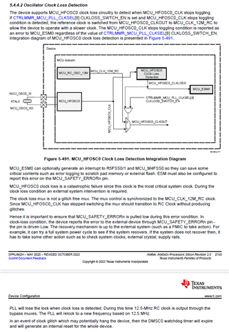
    Oscillator Clock Loss Detection

    Observation clocks

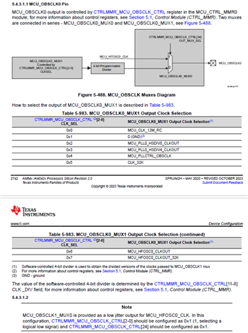
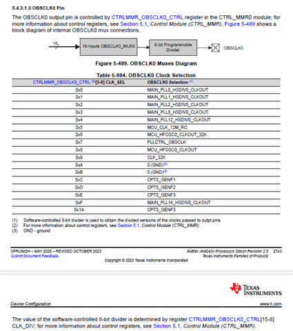
    One more observation we had capture, we monitored the OBSCLK0 output using an oscilloscope. We mapped the OBSCLK0 pin to output MCU_HFOSC0_CLKOUT:

    • When the 25 MHz external clock is active, we observe 25 MHz on the oscilloscope.
    • After the fallback, the output changes to 12.5 MHz.
    • However, when the external 25 MHz clock is re-enabled, the oscilloscope again shows 25 MHz, but the processor continues to run on the internal 12.5 MHz clock.

    Regards,

    Sreenivasa

  • Hi Board designers, 


    Refer below inputs for AM62A3-Q1: Oscillator Clock Loss Detection. This should be same for all the AM62x devices. 

    If MCU_PLL_CLKSEL_CLKLOSS_SWTCH_EN is set, when HFOSC0 stops, will it automatically switch to CLK_12M_RC and output to the MCU_ERRORn pin at the same time?
    [TI] >> Yes.


    Which register can be used to determine that it has been automatically switched to CLK_12M_RC?
    [TI] >> You can read ESM event register WKUP_ESM0_ESM_LVL_EVENT_IN_13


    Does the oscillator return to HFOSC0 when a warm reset?
    [TI] >> I am not sure if I understand this question. When HFOSC0 starts switching again the reference clock will be automatically switched to HFOSC0 clock.


    Will it switch to CLK_12M_RC even if HFOSC0 is not oscillating at cold start?
    [TI] >> By default MCU_PLL_CLKSEL_CLKLOSS_SWTCH_EN is set to ‘0’. So at cold start, if HFOSC0 is not switching then the mux will not switch to CLK_12M_RC. If HFOSC0 is not switching during cold start, the device will not boot-up.

    Accuracy of the MCU_RC_OSC_12M

    https://e2e.ti.com/support/microcontrollers/arm-based-microcontrollers-group/arm-based-microcontrollers/f/arm-based-microcontrollers-forum/1431627/am2431-accuracy-of-the-mcu_rc_osc_12m

    (+) [FAQ] AM6422: How to Switch Back to External Clock After Clock Loss Detection - Processors forum - Processors - TI E2E support forums

    We tried the power cycle of AM64x and observe 2 cases:
    1. Ocsilator Disabled: AM64x doesn't boot up.
    2. Ocsilator Enabled: AM64x runs on 25MHz clock.

    We modified the config to enable clock loss detection as mentioned in above post. Then we did the warm reset of AM64x and observe the following scenarios: 
    1. Ocsilator Disabled. Clock losss detected and after watchdog reset / warm rest AM64x runs on 12.5 MHz.
    2. Ocsilator Enabled: AM64x continued running on 12.5MHz not switched to 25MHz.

    We monitored MCU_SAFETY_ERRORn pin, during clock loss detection pin status changed from HIGH->LOW. However, there is no transition detected when 25MHz clock available again.

    I added the inputs from out reset expert:

    The expectation is that the fault is routed to the ESM, and some external circuit would generate a power cycle or cold reset so the system can recover.  I think this is the only way the clock loss detection circuit would reset the detection.  Also, MCU_PORz is the only way CLKLOSS_SWITCH_EN bit gets reset.  So a warm reset will not help here, and that is why they observe the 12MHz_RC still clocking the processor after a warm reset


    The RC clock backup is not available immediately after PORz because of the default value of CLKLOSS_SWITCH_EN.  There is some setup that needs to happen anyway, in that the error needs to be routed to the ESM to trigger the ERROR signal, so that an external can do something about it (power cycle the device, for example).  When all that is setup, the RC clock will clock the device after a fault, but it is only intended to keep the ESM alive to generate the appropriate ERROR signal.  It is not expected that the device will operate fully.


    On a cold reset, if the 25MHz is not available, the device will not boot.  Even if the clock loss detection circuitry works at that point, the CLKLOSS_SWITCH_EN defaults to 0 as mentioned previously, so the mux will never switch to the RC clock.  Even if it would be able to switch, the ROM does not support booting with that input frequency.

    Regards,

    Sreenivasa

  • Hi Board designers, 

    Information related to clock input frequency increase.

    Q1. Will the all clock (MCU_SYSCLK0 for example) in the device be doubled?

    A1: Oscillator clock being the reference clock, if it is doubled, clocks in the system will be doubled.


    Q2. If the device is running with Max frequency (800MHz), will the device run with abnormal clock?
      Or will the device stop running?

    A2: A clock that does not match expectation (higher than maximum frequency in this case) does not *stop* the device from running. The functionality will be unpredictable as there could be many logic paths that cannot meet the higher frequency.

    Regards,

    Sreenivasa

  • Hi Board designers, 

    Query regarding Spread Spectrum input:

    Does MCU_OSC(25MHz) support spread spectrum clock oscillators?

    Please refer to the device specific data sheet for the crystal requirement or for using external LVCMOS clock input.

    SS clock input is not supported.

    (+) AM625: external and internal spread spectrum oscillator support - Processors forum - Processors - TI E2E support forums

    1. Do AM62x processors support external clock generator or do they support ONLY crystal oscillator?

    2. If external clock generator is supported, does it support SS oscillator also? I have a problem with USB Device mode communication when I use SiT9005AC-13-18NH25.000000 as oscillator. Other peripherals like LPDDR4, SD card interface and eMMC flash work in general.

    3.  Based on this link (https://e2e.ti.com/support/processors-group/processors/f/processors-forum/1358154/am625-pll-spread-spectrum-modulation), internal SS feature is not supported in AM62x devices. Is it still correct or is it supported now?

    1) Yes. You can use a 1.8V LVCMOS clock source rather than a crystal circuit. However, the current datasheet does not define the MCU_OSC0 LVCMOS Digital Clock Source Requirements. We will be adding these requirements to the next revision of the datasheet. For now, please refer to the "MCU_OSC0 LVCMOS Digital Clock Source" section of the AM62Dx or AM62Px datasheets. The requirements for AM62x will be the same.

    2) An external 1.8V LVCMOS source is supported, but not a Spread Spectrum source. As mentioned above, please follow the requirements defined in the "MCU_OSC0 LVCMOS Digital Clock Source" section of the AM62Dx or AM62Px datasheets.

    3) That is correct. SSC is not currently supported on AM62x. We may support SSC on the PLL that sources the DSS peripheral in the future, but there are no plans to support SSC for any other PLLs.

    Regards,

    Sreenivasa

  • Hi Board designers, 

    Inputs related to IBIS model for Xi

    NC is the expected connection for the AM64x, AM62x, AM62Ax, AM62Px and AM62L family of processors. This is the crystal or oscillator input. We do not provide any IBIS models for the clocking section IP of the processor.

    https://e2e.ti.com/support/processors-group/processors/f/processors-forum/752136/tms320c6746-ibis-model-for-l19-oscin-pin/2782761

    I checked a couple of other IBIS files available on TI.com, and they also do not provide model data for the oscillator inputs (even if used as an clock input from some LVCMOS oscillator source instead of a crystal).

    I suspect the reason is because these clock/crystal inputs are analog in nature, but I will follow up with our IBIS expert. IBIS files are meant for IO buffers.

    This NC for OSCIN/CLKIN pins is consistent with other devices.

    https://e2e.ti.com/support/microcontrollers/c2000-microcontrollers-group/c2000/f/c2000-microcontrollers-forum/274626/f2812-pgf-ibis-model-clk-is-nc-signals

    We checked with our Design team on this and got the following reply:

    "We do not provide IBIS models for power/ground/Oscillator pins.  Usually SI simulations are significant for drivers.  X1 being a receiver may be modeled as a simple cap".  

    Just to clarify further, SI simulations are significant primarily for drivers. i.e. Signal integrity simulations are useful only for I/O pins and not for input-only, clocking pins like X1.  

    OMAP-L138: OSCIN (pin L19) missing in IBIS model?

    OSCIN input (pin L19) is missing in OMAP-L138 IBIS model. Do we have updated IBIS file?
     
    Or is OSCIN not required for IBIS? Having said this should customer try to find an option on his compilation tools to ignore these pins…

    Generally speaking, OSC inputs are not simulated, especially if an actual crystal is used.  IBIS does not simulate analog inputs.

    Regards,

    Sreenivasa

  • Hi Board designers, 

    Inputs related to Crystal ESR requirements:

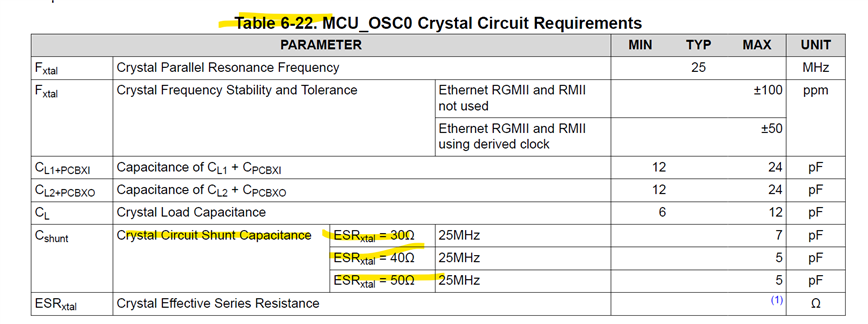
    From the datasheet of AM62A7 table 6-22 it is mentioned here what are the limits for shunt capacitance based on the crystal ESR. The examples provided are 30,40 and 50ohms. 

    Does this mean these are the only acceptable ESR values?

    Can we use a crystal with 80ohm ESR with a shunt capacitance of 2pF?

    Q1: That is correct, as described in the table note associated with the maximum value of the "Crystal Effective Series Resistance" parameter.

    Q2: Maybe, but we do not have any data points for crystals with an ESR greater than 50 ohms. Most crystal manufactures offer a service for validating your specific design with one of their crystals to confirm it provides enough margin for proper oscillation. I suggest you have your crystal circuit validated by the crystal manufacture if you select a crystal with an ESR greater than 50 ohms. Another option would be to look at crystals in larger packages since they typically have a lower max ESR.

    Note: You must consider the total shunt capacitance applied to the oscillator pins when designing your crystal circuit, which includes the crystal shunt capacitance, PCB trace shunt capacitance, and the AM62Ax package contribution defined in datasheet parameter "XI to XO Mutual Capacitance".

    Therefore, the total shunt capacitance will be larger than the shunt capacitance defined in the crystal datasheet.

    You need to be careful using values in crystal datasheets found on the internet because in most case the datasheet represents an entire family of crystals with a broad range of frequency options. Typically, the higher frequency crystals within a family will have significantly lower ESR than the lower frequency crystals, and publicly available datasheets will publish the worst case ESR for the entire family of crystals. You should ask the crystal manufacture to provide a part number specific datasheet if you want to know the max ESR of the specific crystal you selected.

    Could you help to review the following 25MHz crystal from our preferable vendor is OK for MPU (AM62L) application ?

     CX2016FB25000B0FZZH1

    Frequency error 10PPM
    Frequency stability 20PPM
    Temperature range -40 to +85C 
    load capacitance 6 pF
    ESR 100 ohm  
    Drive level 100uW
     www.mouser.com/.../CX2016FB25000B0FZZH1

      In addition, you mentioned we would need to populate the 2 caps and the 3 resistors, could you please refer me to the guide about 3 resistors?"

    There is a good chance this crystal will work fine with our oscillator, but technically its ESR is too high to meet the datasheet requirements. Our datasheet ESR limit is a function of crystal circuit shunt capacitance, where a higher ESR can be used when the crystal circuit shunt capacitance decreases. This crystal datasheet defines has a much lower shunt capacitance than we typically see in a crystal datasheet. Therefore, our datasheet does not show an ESR/Shunt capacitance combination that can be used to decide if this crystal is acceptable. We would need to ask our analog design team to evaluate the combination of ESR (100 ohms) and crystal shunt capacitance (less than 1pf) to see if it is a valid combination.

    In the past we have suggested resistors to be placed in the crystal circuit of prototype boards to enable crystal circuit performance checks before going into production, but this oscillator has an internal Automatic Gain Control (AGC) amplifier that eliminates most of the uncertainty associated with crystal selection as long as you select a crystal that meets or datasheet requirements.

    The "WKUP_OSC0 Crystal Implementation" figure shows a schematic of crystal circuit component connectivity, and the "WKUP_OSC0 PCB requirements" figure shows the expected PCB layout.

    e2e.ti.com/.../5031483

    Crystal power dissipation depends on crystal circuit variables that need to be considered. The high frequency oscillator implemented in AM62x has an Automatic Gain Control (AGC) circuit that adjusts its drive strength to achieve resonance, which is another variable associated with crystal power dissipation. Therefore, it is not possible for TI to define a power dissipation parameter for every crystal circuit implementation. The system designer would need to measure the voltage across their crystal circuit and use the following formula to calculate power dissipated in the crystal.

    The crystal power dissipation can be calculated by the following formula.

    Pxtal = 0.5 ESR (2 π Fxtal CL Vxtal)2, where ESR is the Effective Series Resistance of the crystal, Fxtal is the resonate frequency of the crystal, CL is the capacitive load of the crystal circuit, and Vxtal is the peak-to-peak voltage across the crystal.

    Regards,

    Sreenivasa

  • Hi Board designers, 

    Inputs related to Clock not oscillating when using Crystal 

    (+) AM2431: AM2431 – RESETSTATz remains LOW, no clock observed on MCU_OSC pins - Arm-based microcontrollers forum - Arm-based microcontrollers - TI E2E support forums

    After removing R140 (pulldown for X0 when poscillator is used), the clock is now generated correctly. I am able to observe both RESETSTATz and MCU_RESETSTATz transitioning to the HIGH state. I also performed a JTAG connection test, and it is working without any issues.

    Thank you to you and others in this thread for the guidance and assistance.

    Please find the attached waveform/image for your reference.

    Additionally, could you please review my DDR, eMMC, OSPI, and USB interface circuits, along with their associated reset circuits. This would be helpful for the next stages of bring-up.

    Regards,

    Sreenivasa

  • Hi Board designers, 

    Inputs related to crystal connections and MCU_OSC0_XO connection when oscillator is used


    During measuring the MCU_OSC0_XO signal there was a deviation with the specification in the data sheet observed. The MCU_OSC0_XO signal only reaches a max. level of ~800mV and at the start up you can see that the signal is not symmetric. In comparison to Figure 7-17. in the data sheet the high level of the oscillation should be at ~ VDDS_OSC0 (min.) VDDS_OSC0 =1.8 V.
    Is there any explanation or reason for this behaviour? The Crystal Circuit is implemented like it is mentioned in the requirements.
    We do not recommend measuring the Xo. Alternatively, you could measure the buffered clock output on the WKUP_CLKOUT0
    – WKUP domain CLKOUT0 output. pin.

    Please verify the load cap used vs required for the crystal. Consider the stray cap of ~4 pF.
    Do you have any series resistor between the SoC and the crystal. We do not recommend using any resistor. if there is some resistor, pls change to 0R.
    In case you would want to probe the crystal, the recommendation is to use a passive x10 probe rather than the FET probe
    I've measured the buffered clock output on the WKUP_CLKOUT0 and now it has 3.3V, 25 MHz and a good signal quality.

    https://e2e.ti.com/support/processors-group/processors/f/processors-forum/1582085/am6442-about-mcu_osc0-internal-oscillator-clock-source/6101092

    e2e.ti.com/.../am67-mcu_osc0_xo-and-wkup_lfosc0_xo-pin-termination
    Are MCU_OSC0 and WKUP_LFOSC0 receiving a LVCMOS clock input? If yes, please follow the datasheet requirement to ground the *_XO pins. The *_XI and *_XO pins are capacitively coupled as differential signals to drive the respective OSC clock into the device. Connecting *_XO to VSS makes the receiver act a single-ended comparator.
    When using a crystal circuit, you should implement the circuit as shown in the figure titled "MCU_OSC0 Crystal Implementation". No external resistors required.
    The XO is connected to VSS when using a LVCMOS clock source because the internal reference clock is derived from a differential input buffer that requires a difference voltage across XI and XO, so it is necessary to connect XO to ground when only applying a signal to XI.
    TI recommends following the datasheet guidance to minimize noise on the differential receiver. We cannot guarantee the performance for the oscillator outside datasheet guidelines, and that configuration has not been validated by TI. There is a chance it could work with *_XO left open but we would not recommend going to production with that.

     RE: AM2432: MCU_OSC0_XI和MCU_OSC0_XO电平 

     RE: AM2432: MCU_OSC0_XO termination 

    AM335x related
    RE: AM3352: The MPU may fail to boot into the OS, causing screen flickering. When performing a Power Reset... 

    During reset, on some of the units the display flickers. If customer changes the crystal to oscillator, the issue is resolved. Customer is pushing for a root cause.
    There is a errata for the crystal grounding.
    Is it Ok for customer to use the crystal following the errata or is the recommendation to use an oscillator as clock source.

    The customer is ultimately responsible for design a robust system. They need to use a solution that is robust in their system design. A solution that works for one customer may not work for another.
    Many customers are able to use the crystal circuit with the updated ground connection without any issue. However, some customers have a very noisy system design that allows noise to couple into the crystal circuit and the coupling of noise into the crystal circuit generates glitches on the internal reference clock. Glitches on the reference clock can effectively over-clock internal state-machines, which cause unexpected behavior.
    The reference clock signal generated by the crystal circuit has a slow rise/fall times relative to the rise/fall time provided by an LVCMOS oscillator. The slow rise/fall signal from the crystal circuit has a higher susceptibility to noise creating non-monotonic events on the signal transition as it passed though the switching threshold of the input buffer. It is difficult for noise to produce non-monotonic events on the transition of the faster rise/fall signal generated by an LVCMOS oscillator.
    The customer has two choices. The first choice is, determine the noise source / coupling mechanism into the crystal circuit and eliminate the noise or coupling. The second choice is, use the less noise susceptible LVCMOS clock source solution.

    Most PCB designers know all of the crystal circuit components should be placed very close together and near the oscillator terminals. When the PCB is designed this way, the crystal component ground connections would be very close together, so we expected each ground connection to be a direct connection to the digital ground plane (VSS). It is not necessary to connect them together with single point connection to ground.

    General Guidelines

    I will define the crystal component grounds to clarify this point. There should be three or four crystal component grounds.
    1. The first ground connection is for C1
    2. The second ground connection is for C2
    3. The third ground connection is for the respective oscillator ground (VSS_OSC or VSS-RTC).
    4. This fourth ground is an optional connection to ground for the crystal package shield if the crystal selected has a shield.

    AM335x - Advisory 1.0.30: OSC0/OSC1 noise immunity
    You mentioned the customer ‘tied the crystal to ground’. I need to understand what this comment means.
    Does this mean they only tied the crystal package/case to ground or did they tie the VSS_OSC/VSS_RTC terminal and all crystal component grounds to the nearest PCB digital ground?
    Advisory 1.0.30 recommends the VSS_OSC/VSS_RTC terminal and all crystal circuit grounds should be connected to the nearest PCB ground.
    I have never seen a case where this recommendation has caused more noise to couple into the crystal circuit.
    We were not able to measure the noise because adding a probe to the crystal circuit influences noise coupling. We reached our conclusion based on two weeks of testing multiple PCB designs with various noise sources.
    We do not make any specific recommendations related to crystal package, but all the boards we tested were using small 4 terminal ceramic SMT crystals and two of the terminals were also connected to the nearest PCB digital ground.

    A 1.8 v digital clock source can be used to replace the crystal circuit and it will be much more difficult to couple noise into this clock source. The digital clock source has fast rise/fall edges that transition through the input switching threshold very quickly and is not as susceptible to noise while the crystal circuit produces a near sine-wave signal that slowly transition through the input switching threshold.


    AM3358: AM335x OSC0 Crystal Circuit Load Capacitance 

    e2e.ti.com/.../system-time-jump-problem-and-am335x-advisory-1-0-30
    The oscillator input buffer has a switching threshold voltage where the output will change states as the voltage applied to the input crosses the threshold. The voltage applied to the oscillator input buffer is a slow changing sinusoidal signal when using a crystal circuit as the reference clock. Noise coupled to this slow slew rate signal may cause the output of the oscillator input buffer to toggle several times as the signal slowly crosses the switching threshold. If this occurs, the internal clock signal will think these unexpected toggles are real clock toggles. However, these unexpected toggles are much higher in frequency than the real clock toggles. These much faster toggles will violate internal circuit timing and in some cases may cause the circuits to perform unexpected operations. For example, portions of the RTC counter circuit may see these fast toggles and respond properly while other portions of the RTC counter circuit do not see the fast toggles. In such a case, the RTC counter may not function as expected and do very unpredictable things like counting backward.

    If this happens, any internal circuits being clocked from the oscillator output may perform unexpected operations. In most cases the DPLLs acts like a filter and circuits being clock from the DPLLs never see these unexpected toggles. We saw one case of a DPPL performing an unexpected operation while debugging this issue, but as mention above any circuit being clocked from the oscillator could perform unexpected operations when excess noise is coupled to the oscillator input signal.

    This issue is completely eliminated if you use a fast slew rate clock source like you get from an LVCMOS clock source. It is also much harder to cause this issue on the Master oscillator vs the RTC oscillator because the slew rate of the 19.2 MHz - 26 MHz oscillator is much faster than the 32.768 KHz oscillator.

     RE: AM3352: VSS_OSC and VSS_RTC connection 

     AM335x Power rails GND connections 

     VSS_OSC and VSS_RTC connection to PCB ground 

     RE: The connection of VDDS_RTC on TMDSSK3358 

    The VSS_OSC terminal has a higher impedance connection to the internal ground of OSC0 that the VSS terminal, so the decoupling capacitor is not as effective as it could be if it were connected VSS rather than VSS_OSC.

    The TI EVM has the same mistake and we have not had any reports of this causing a problem. However, the EVM is normally used in a lab and may not be exposed to the same environmental conditions (like temperature variations, external electrical noise, and etc) as a production product.

    Based on my experience, I would be much more concerned with the issue described in Advisory 1.0.30.

     RE: AM335X Peripheral PLL freq. increases by +25% 

     RE: AM335x display PLL configuration problem - TFT flickering 

     AM335x: What are the implications of connecting VSS_OSC to VSS in a system that uses an external crystal 

    AM335x - Advisory 1.0.30: OSC0/OSC1 noise immunity

    A 1.8 v digital clock source can be used to replace the crystal circuit and it will be much more difficult to couple noise into this clock source. The digital clock source has fast rise/fall edges that transition through the input switching threshold very quickly and is not as susceptible to noise while the crystal circuit produces a near sine-wave signal that slowly transition through the input switching threshold.

    https://e2e.ti.com/support/processors-group/processors/f/processors-forum/270632/about-am335x-dm-timer/1032586#1032586


    High frequency digital switching current flowing through inductive substrate traces and bond wires that connect the silicon die to the PCB ground produces a few milivolts of ground noise on the die relative to the PCB ground.

    When the crystal circuit is referenced to the PCB ground and the oscillator input is referenced to the die ground, the oscillator input will see this high frequency ground noise summed with the crystal output voltage. This can potentially increase clock jitter since the crystal output voltage is a relative slow changing sinusoidal signal and the high frequency ground noise can cause the oscillator input to see slightly shorter or longer clock cycles.

    The Kelvin ground allows the crystal circuit ground to be at the same potential as the die ground and reduces the oscillator input noise.

    There should not be any change in power supply consumption.


    RE: Questions regarding AM3358 DPLL Power Supply Requirement and the Input Clock 

    The LVCMOS digital clock source connected to the OSC0 XTALIN terminal should be powered by the same source as connected to VDDS_OSC terminal.
    The LVCMOS digital clock source connected to the OSC1 RTC_XTALIN terminal should be powered by the same source as connected to VDDS_RTC terminal.

    Both VDDS_OSC and VDDS_RTC terminals have a recommended nominal operating voltage of 1.8 volts.

    The OSC0 VSS_OSC terminal and OSC1 VSS_RTC terminal should be connected to the digital ground when using external LVCMOS clock sources.

    e2e.ti.com/.../583015
    As I now understand it on the ZCZ package, both the main oscillator, OSC0, and the external RTC oscillator, OSC1, have floating Kelvin ground terminals, VSS_OSC and VSS_RTC respectively. Can you please recommend how to wire VSS_RTC when OSC1 is not being used.
    Each Kelvin ground terminal should be only connected to the respective external crystal components as shown in the OSC0 Crystal Circuit Schematic data manual figure when a crystal is connected to the respective oscillator.

    Each Kelvin ground terminal should be connected to the PCB ground when an LVCMOS digital clock source is connected to the respective oscillator.

    When not using the RTC oscillator (OSC1) the VSS_RTC Kelvin ground terminal should be connected to the PCB ground.

     The connection of oscillator on TMDSSK3358 

    If the oscillator package has ground terminals, those terminals should also be connected to the respective Kelvin ground terminals (VSS_RTC or VSS_OSC).

    The decoupling capacitor connected to the VDDS_OSC (R11) terminal should not be connected to the GND_OSC0 net which is connected to the VSS_OSC (V11) terminal as shown in the schematic. This capacitor should have been connected to VSS.

    Regards,

    Sreenivasa