Other Parts Discussed in Thread: OPA365, INA240
Good day Ti,
I build a new motor controller board with low side current sensing and the OPA365 as op-amps. On the op-amp output there are heavy oscillations. All other waveforms like the phase or the gate voltages looks very good, there is almost no ringing.
I think I know where they come from but I’m not sure, if there is something I can do against it and wanted to ask you if you have any ideas or comments to this.
Because of the inductance of the shunt resistor and the supply path I added a 1uf capacitor between drain of the high-side fet and source of the low-side fet to suppress the initial voltage pulse on the source of the low-side fet.
This capacitor reduces the initial voltage pulse, but I think it is forming an LC-Circuit with the inductance of the shunt and supply path and this causes the oscillations. Do you also think that is the cause or is there something that I didn't think of?
Here is a picture what I mean:
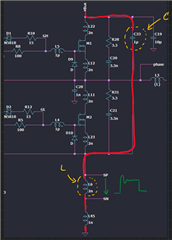
But when I remove the Capacitor (in the picture above, the yellow C) between HS-FET drain and LS-FET source, the ringing reduces a lot, in simulation and on the real board. On the other side, when I remove this capacitor I have a larger voltage spike on the source of the LS-FET, which could be damage the DRV. Should I consider using a lower capacitance? At the moment it is 1uF.
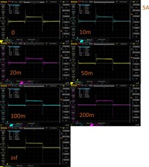
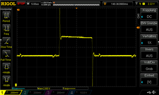
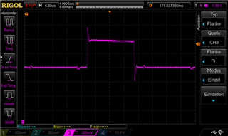
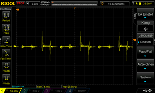
Here are two pictures of the opamp output when measuring the current, it’s only about 4A in this picutures:
This is with HS-Drain – LS-Source capacitor:
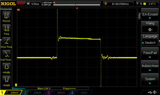
This is without HS-Drain – LS-Source capacitor:
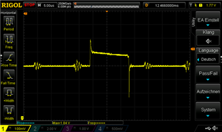
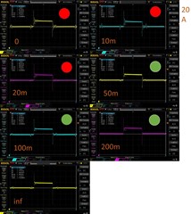
And here are two pictures from the voltage between ground and LS-Source:
This is with HS-Drain – LS-Source capacitor:
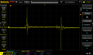
This is without HS-Drain – LS-Source capacitor:
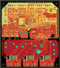
Most of the time I used inline sensing with an INA240 for example where I don’t have this problem. It would be nice to know if there are some things that help would help in this case. I can’t change the inductance of the shunt, I already uses shunts with low inductance, and I think the layout should be ok, there are some pictures at the bottom and all schematics.
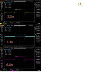
What I’ve done so far, I changed the input filter of the op-amp and the oscillations reduced many.
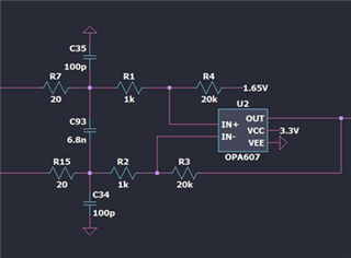
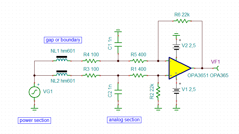
In the picture below you can see the circuit before I change the filter. The values in the picture are the real values.
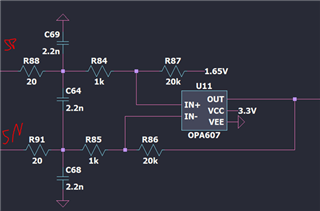
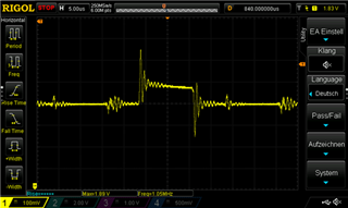
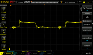
Here is the output of the op-amp on the board: (It looks much worse if C69 and C68 are not placed)

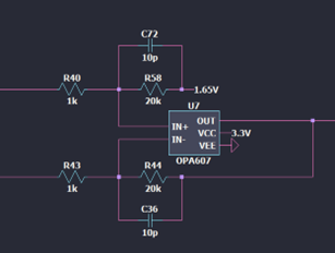
With the values below, the ringing reduced a lot with this:
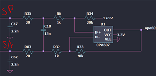
As you can see here:
But this reduces the cutoff frequency to about 400kHz, I won’t go lower. How do I determine the minimum bandwidth for an op-amp used in low side current sensing (for inline it’s clear for me). The OPA365 has definitely enough bandwidth. I saw a lot of rule of thumb formulas but on what does it really depend? Do you have an app note for this?
My sampling time of all three phases is about 150ns-500ns depends on the MCU. PWM frequencies are between, 10kHz and 40kHz. Minimum on time of the low side fet of duty is 2-3us min and usually 5us. Sampling happens in the middle of the on time from the LS-FET at which point the voltage should already have settled to a reasonable value.
di/dt is about 80A in 30ns-40ns on the shunt resistor. 80A is the maximum current to measure, there I have about 80mV on inputs of the op-amp (1mOhm shunt, gain is 20). This is a dv/dt of 2V/us.
What I didn’t try so far what this kind of filter, maybe there is less ringing, but the settling time would be the quite same I think.
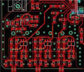
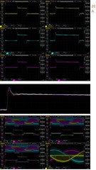
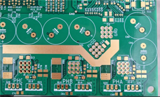
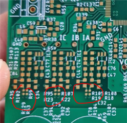
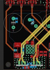
Here are the layout and schematics:
op-amp circuit: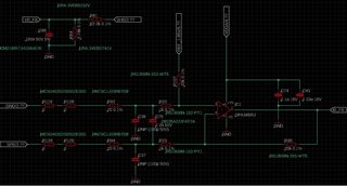
op-amp layout: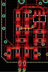
routing of the sense traces:
Best regards and thank you in advance,
Daniel