This thread has been locked.

If you have a related question, please click the "Ask a related question" button in the top right corner. The newly created question will be automatically linked to this question.

OPA2835: Request for suggestions for using Attenuator for Voltage signal

Part Number: OPA2835
Other Parts Discussed in Thread: ADS131M03-Q1, OPA835, ADS131M03, OPA392, LM2904, LM2902, TLV9001, TLV9002, LM2904B, LM2904LV, LMV321, INA181, INA351, TLV333, TLV07, XTR117, XTR115, XTR116, INA146, INA149, INA148, INA132, INA213, INA185, TMP61, ADS1120

Dear community members,

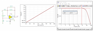
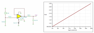
I recently came across the OPA2835 in the RUN-Package, which features integrated gain setting resistors capable of achieving various inverting attenuations (-0.1429, -0.1875, -0.25, -0.33, -0.75). I was wondering if anyone could recommend cost-optimized alternatives of similar OpAmps that also include built-in gain setting resistors for attenuation.

Additionally, if anyone could provide a reference design that could assist us in our final circuit design, it would be greatly appreciated.

Our specific requirements involve attenuating 0-5V and 0-10V signals to:
1) A 0 to 3.3V signal for our ADC on the MCU
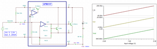
2) A -1.2 to 1.2V signal for the ADS131M03-Q1 ADC (or single-ended input to this ADC)

The solution we are developing is a temperature & Current sensor-based Data Acquisition module for Micro & Small Industries in India and is a highly cost-sensitive application that requires maximum accuracy that we can afford. Our target error in the driver circuitry is 0.25%, better accuracy would further help improve our Condition Monitoring insights.

Any guidance or suggestions would be highly valued.

Thank you.

Regards.

  • Hello Shreeneet,

    I have clarifying questions:

    1. Are you looking for a single amplifier with integrated resistors, or a dual-amplifier device with integrated resistors?  Only the OPA835 in the RUN-package includes integrated gain-setting resistors; the OPA2835 in the RUN and RMC packages does not have any integrated resistors.  Please clarify if your application requires a single or dual amplifier.

    2. You mention cost-optimized; the OPA835 RUN (with integrated resistors) has a $1ku price of ~$1 USD.  Is there a target BOM cost or threshold price you are looking for?  Integrated components and overall complexity typically result in higher cost than simpler amplifiers.

    3. Is the need for integrated components strictly due to tight spacing requirements?  Could a lower-cost op-amp with discrete resistors around it fit in the sub-circuit footprint in your design?  If the need for built-in attenuation resistors is found to be greater than a target BOM cost, you may be best suited for the OPA835RUN.  If you have more relaxed spacing requirements, it may be easier to recommend devices in a certain cost range.

    4. What is the bandwidth of the signal being driven into the ADC?  If your concern is high precision, a lower-bandwidth precision part may be a better fit.  The sampling rate of 64ksps results in a Nyquist bandwidth of 32kHz.  The PRAMPs product line may have a broader selection of high precision, integrated resistor products.

    I look forward to hearing back regarding my questions.  Regarding a reference design or support documentation, I will wait until we finish discussing amplifier choice before looking up amplifier-specific reference design or app notes.

    Best,

    Alec

  • Hello Alec,

    Thank you for your response. Here are some further clarifications regarding our requirements:

    1. A single amplifier with integrated resistors would be suitable for our application. We appreciate you pointing out that the OPA2835 lacks integrated resistors.
    2. Our target price per channel is a maximum of $2, which includes all components in the signal chain up to the ADC. The ADC itself costs approximately $1.2 for our minimum order quantity (MOQ) of 250 units per quarter.
    3. We are open to a more relaxed spacing solution with resistors. Currently, discrete resistors (precision 0.1%, metal film, 25PPM/'C) cost around $0.5 per array of 2 in our MOQ range. We are considering Vishay Beyschlag resistor solutions, but we would appreciate any guidance on alternatives.
    4. Our required bandwidth for current monitoring is a maximum of 10kHz. However, for temperature monitoring, the bandwidth shall be much lower.

    To provide more context, we are developing a condition monitoring platform with a target price of $60. It currently includes 3 temperature sensing channels and 3 current sensing channels. Of which we are using MCUs inbuilt ADC for temperature sensing, & ADS131M03-Q1 for Current sensing. We want to ensure the device remains scalable and flexible for adding more channels in the future, plan is to add multiples of ADS131M03 in Daisy Chain for up to additional 6 channels. Our target customers are micro and small-scale industries in India, extremely cost sensitive atm for even entry levels CbM applications. STM has been very supportive by providing us with favorable pricing for the G474 series MCU, which offers the required processing power we need.

    Our future plans involve adding pressure, voltage, and vibration sensing (with a maximum of 1024-size FFT) once we start generating value for our customers with the current setup. We will be using I2C/SPI for high BW & high-precision measurements including vibration. And require a good-quality ADC signal chain.

    Thank you for your assistance.

    Best regards,
    Shreeneet

  • We are looking for a high-precision signal chain that can remain affordable. And our background & expertise is in Model development & Fracture mechanics, hence we may not have the best insights about Analog circuitry, so TI's vast amount of design resources & reading material have been extremely helpful so far to us.

    1. Input Signal Voltage: 0-5V & 0-10V | ADC input range: +-1.2V & 0-3.3V
    2. Input Signal Current: 4-20mA | ADC input range +-1.2V & 0-3.3V
    3. Recommendation for cost-optimized lo error unity gain buffer for improving input impedance

    We have currently selected TMP6131ELPGMQ1 for temperature measurement & will interface it directly with the MCU ADC.

    Following is the Current Sensor Specifications we plan to use with ADS131M03-Q1 ADC.

    The maximum bandwidth of up to 10kHz for current & voltage monitoring, for any other sensors channels BW shall be around 5kHz range maximum. And we plan to select I2C/SPI-based sensors when high BW and high Precision sensing requirements arise.

  • Hello Shreeneet,

    I appreciate you providing the high level of detail around your application and amplifier needs.  Based on the sampling rate of 64ksps, I do think we should check over with the precision amplifiers team.  I am adding them onto this thread, please allow a bit of time for their team to read and work on your needs.

    Best,

    Alec

  • Shreeneet,

    1. We discussed a possible signal chain previously:  ADS131M03 signal chain
    2. Is this the same project?  For the previous question the input range was ±12V to 1.2V.  In this case the range is a little different but the ADC is the same.  We can easily modify the topology to accommodate any input signal range.  Let me know if you want help with a specific range.
    3. Here are some cost optimized amplifiers with automotive qualification and ±15V supply capability:  cost optimized automotive precision devices 
    4. Here are some general purpose amplifiers that are automotive qualified and have ±15V supply capability.
    5. The difference between "general purpose" and "precision" is the offset voltage specification.  Precision Vos <1mV, general purpose Vos > 1mV.  General purpose will tend to have lower cost.

    Let me know how I can help.

    Best regards, Art

  • Hello Art,

    Thanks for your response, the previously suggested solution is going beyond our project budget, and unfortunately, the OPA392 is currently out of stock. While searching for alternatives to the OpAmp, we discovered the OPA835 RUN package, which features an inbuilt Attenuator Resistor divider. This prompted us to reach out to the Community for further guidance via this post.

    To optimize costs and minimize inventory, we are aiming to use the same ADC - ADS131M03-Q1 for multiple applications. We are seeking a lower-cost signal chain reference design that we can keep using in our circuits with an accuracy of approximately 0.25% error.

    It would be ideal if Texas Instruments has a cost-optimized version of built-in attenuating resistors like in the OPA835 RUN package. However, we are open to utilizing an external resistor network with a Buffer OpAmp for cost optimization purposes.

    We would greatly appreciate your guidance on the following aspects to help us complete our signal chain designs:

    1. Input Signal Voltage: 0-5V and 0-10V | ADC input range: ±1.2V and 0-3.3V
    2. Input Signal Current: 4-20mA | ADC input range: ±1.2V and 0-3.3V
    3. Recommendations for a cost-optimized, low-error unity gain buffer design at ADC input to improve input impedance.

    Our maximum required bandwidth is 5kHz for all sensors & 10Khz for current & voltage sensing, any sensor that shall demand higher bandwidth, we have decided to use an I2C/SPI digital solution & avoid the ADC signal chain altogether.

    Thank you for your guidance.

    Regards

  • Shreeneet,

    1. For your high voltage input amp, I used the following criteria:
      1. Automotive qualified
      2. Lowest cost option
      3. 1MHz GBW
      4. General purpose type: Vos>1mV (lowest cost amplifier subcategory)
      5. Max Supply rating >= 36V for input amplifier
      6. high voltage input amp options Q1 
      7. I chose LM2902, or LM2904
    2. For your ADC amplifier options, I used the following criteria:
      1. Automotive qualified
      2. Lowest cost option
      3. 1MHz GBW
      4. General purpose type: Vos>1mV (lowest cost amplifier subcategory)
      5. Min Supply rating <= 2.4V for ADC drive
      6. Rail-to-rail for ADC drive
      7. low voltage adc drive 
      8. I chose: TLV9001 (or dual TLV9002)
    3. There are many other options.  Of course, when you target low cost some performance may suffer.  Let me know if you have other key specifications that are important.  My main goal was to make sure that to make sure that the input and output swing was not limited by common mode or output swing.  This is why I chose rail to rail for the ADC driver.  I am also designing the circuit so that the ADC cannot be overdriven as the amp supplies are limited to safe levels.  I selected 1MHz GBW as you mention signals in the 10kHz range so 1MHz gives good margin and generally good noise performance.
    4. Here is the updated document to include the 0-5V and 0-10V | ADC input range: ±1.2V and 0-3.3V options.  I kept the original circuits the same but you can substitute the new amplifier options:  adc drive translation options.pdf
    5. Regarding the 4mA to 20mA receiver.  This translation can be done in multiple ways.  One simple approach is the drive the current signal into a resistor to ground.  In other cases the resistor cannot be connected to ground but is sensed with a DIF-AMP.  Which option do you need?
    6. Here are the TINA SPICE files:  single to dif 0V to 10V to 0 to 3p3.TSC,single to dif 0V to 10V to m1p2 to p1p2.TSC,

    I hope this is helpful to you.  FYI.  My team supports the precision amplifier (Vos < 1mV).  I will notify an engineer from the general purpose team as they may have other comments on amplifier options.  I used the general purpose devices as you are looking for low cost options.

    Best regards,

    Art 

  • Hello,

    The LM2904B family will be the best GPAMPs option for cost optimized high voltage operation. Be sure to use the LM2904B, and not the LM2904LV for the high voltage input stage amplifier

    TLV9001/TLV9002 is the best option given the search criteria with RRIO being a requirement. Further cost down solutions exist, but features like the rail to rail input stage will be excluded to realize the reduced cost. Such devices include LMV321 and LM2904LV.

    Art's design is advantageous as the TLV9002 is supply limited such that the ADC cannot be overdriven by the buffer amp. If we pursue a non-RRIO amplifier, the design will get slightly more complex to realize the same function. 

    Please let me know if you have any questions.

    I have included the updated recommended devices in the included TINA simulation.single to diff 0V to 10V to 0 to 3p3.TSC

    Best,

    Jacob

  • Hello Art,

    Thank you for your guidance, which has proven to be very helpful for me and my team. We appreciate the detailed explanation of the decision-making process, as it has improved our understanding. Currently, we are reviewing the designs you suggested and have a few initial questions:

    1. Considering our cost-sensitive application, can we eliminate the need for an ±15V VRef in this circuit? A VRef of 1.2V would suffice, and we can easily accommodate it.

    2. For the 4-20mA loop, we would like to use the ADS131M03-Q1 which has differential input pins, in this case, the Gain of 1,2,4 has 330kOhm input impedance, do we still need to include a buffer?

    We look forward to your insights on these matters.

    Regards

  • Thank you for your response & guidance Jacob,

    Your feedback further strengthens our decision-making.

  • Hello Art,

    We would like to have your feedback on the following configuration for 4-20mA current loop sensing:

    Objective: Design a highly integrated solution for the current measurement system to convert a 4-20mA signal being sampled at 2ksps to a 0-3.3V range suitable for ADC measurement. This is planned to be realized by using an INA181 current-sense amplifier and an 8.2 Ohm shunt resistor.

    The INA181 is configured for a gain of 20V/V. The 4-20mA current signal is converted to a voltage across the 8.2 Ohm shunt resistor. This voltage is then amplified by the INA181. The output voltage of the amplifier is directly proportional to the current flowing through the shunt resistor and ranges from 0 to 3.3V, corresponding to the 0/4-20mA current input.

    The INA181 was selected due to its appropriate gain settings, common-mode voltage range, low offset voltage, and power supply requirements compatible with our system.

    An 8.2 Ohm, 0.5% tolerance resistor was selected as the shunt to ensure accurate current measurements and maintain the output voltage within the range suitable for ADC conversion.

    Questions:

    1. Are we missing something obvious in this configuration?
    2. Assuming the Current loop being driven by 24V & 4-20mA INA181 seems suitable, any low cost techniques to use this for 36V current loops?

    We appreciate your feedback & guidance, thank you.

  • Shreeneet,

    The INA181 may be a good choice for your application.  Here are some things to consider:

    1. The gain error of the device is +/-1%.  Your 8.2 ohm sense resistor has a tolerance of +/-0.5%.  The overall gain error could be as high as 1.5%.  Is this acceptable?  The INA181 is cost optimized.  You can get better accuracy at a higher cost.
    2. Similar to the gain error, the offset is 0.5mV max.  We can find a better offset at a higher cost.  4mA x 8.2 ohm = 33mV.  0.5mV is a 1.5% error on a 33mV signal.

    The accuracy is the main concern that I would have. What overall accuracy you are trying to achieve?

    Art

  • Hello Art,

    Thanks for the feedback. Yes, we would like to choose a better accuracy solution, can you help us with suggestions? our target accuracy is 0.5%. We can select a 0.1% resistor and if required perform one point calibration once.

    This also makes us think, about what should we consider while selecting the device, Typical values or the maximum values as given in the specifications, as considering either of these 2 puts off the error estimations quite off.

  • Shreeneet,

    1. A one point calibration will allow the calibration of offset, or gain error.  It cannot calibrate both out.  How would the one point calibration work?  Normally to calibration offset the inputs can be shorted or no signal is applied.  I assume you are doing an offset calibration only.  This will not help with the resistor tolerance.  This reference explains gain and offset calibration:  calibration video 
    2. Here are some options: ina options
    3. The INA351 looks like a good possibility for you as the cost is low, but the gain error is pretty good.  It uses an internal gain set resistor so you don't need to purchase an external precision resistor to adjust the gain.
    4. Not sure what your power supply requirements are.  You can use this to narrow the search further if the INA351 doesn't meet your requirements.

    Art

  • Hello Art,

    Can you provide a reference design using the INA351 amplifier for sensing a 4-20mA analog current signal and converting it to a 0-3.3V range suitable for an ADC that accepts unipolar input?

    Specifications:

    • Input current signal range: 4-20mA
    • ADC input range: 0-3.3V (unipolar)
    • Target accuracy: 0.2 to 0.5%
    • Required bandwidth: 3kHz maximum
    • Intended for measuring slow-moving physical quantities like temperature.
    • A simple LPF on the input to help mitigate the noise issues.

    We have analyzed the INA351 and identified offset error as the primary source of significant contributing errors. To mitigate this, we plan to implement frequent zero-state averaging in the MCU for calibration. Kindly suggest any other alternative method to calibrate & minimize the offset error of INA351 for 4-20mA measurement application. I strongly believe this design of yours would be widely used as it leverages the highly integrated INA351 in cost-optimized use cases for slow-moving input signals.

  • Shreeneet,

    Here is a power point that goes over two options.  Please confirm which option you want more detailed analysis on.  

    4 to 20 mA reciever.pptx

    Art

  • Hello Art,

    Thank you for the suggestions, being a cost-sensitive application, we would like to minimize the BoM size and use the single supply of 3.3V MCU/ADC power source available onboard to power the 4-20mA circuitry along with possible use any of the 3 available Vref of 2.9, 2.5 & 2.048V delivering upto 6.5mA.

    1. 4-20mA driven by 24V/36V Current Signal Loop
    2. 0-3.3V ADC input range
    3. 3.3V Power Supply
    4. Available Vref from ADC: 2.048V, 2.5V & 2.9V delivering 6.5mA
    5. Error budget 0.2-0.5% maximum

    These are readily available on almost every Mixed Signal MCU-based system that can help minimize the BoM size for such applications.

    Regards.

  • Shreeneet,

    Thanks for the extra info.  It looks like the single supply option should work well for you.  Here are some comments about operation.

    1. In reviewing this further I missed an important error source in the initial recommendation.   The offset voltage is high for this device ( 1.3mV max).  This offset will be multiplied by the gain and show up at the output.  You could potentially calibrate this out.  If it is not possible to do this calibration the 1.3mV will translate to 13mV at the output which is a 32% error on the 4mA, and 6% pm a 20mA signal.
    2. I think a better option is to use a simple op amp buffer.  Sorry I didn't suggest this sooner.  The main two error soruces in this case are:
      1. Tolerance of the sense resistor.
      2. Offset of the amplifier
    3. The recommended amplifier is TLV333.  This is a cost optimized low offset device.  Offset is 15uV max.
    4. With a 135 ohm sense resistor the output will range 0.54V to 2.7V for a 4mA to 20mA signal.  The offset will translate to an error of 0.003% for a 4mA signal and 0.0005% on a 20mA signal.
    5. The main error source would be the resistor tolerance.  A 0.1% resistor will product a 0.1% error for the entire 4mA and 20mA range.
    6. Here is the simulation file:  4 to 20ma tlv333.TSC

    I hope this helps.

    Art

  • Hello Art,

    Thank you for the update, TLV333 is costly for our use case, based on your suggestions, we found TLV07 to be well within our cost as well as error budget. And for the Shunt resistor, we plan to use a 160Ohm resistor that might help us cover the maximum dynamic range of the ADC covering 0 to 3.2V input with 0.1V headroom for any error. Any error of up to 0.2% should be sufficient for our use case.

    Would you recommend some LPF filters for this use case? Also any recommendations & good practices for the use of ESD?

    With use of INA351, performing a Zero Input Condition Calibration must help us minimize this error, right?

  • Hi Shreeneet,

    TLV07 is not low voltage precision op amp. It has Vcm limitation for the 3.3Vdc supply rail.

    TLV E2E 07022023.TSC

    It may work if the resistor is lower to <= 65Ω range. Here is the alternative with LPF filter

    TLV AC response 07222023.TSC

    If you have other questions, please let us know. 

    Best,

    Raymond

  • Hello Raymond,

    Thank you for the design, we realized that TLV07 lacks RtoR input. We found TLV9001 to be within the specifications. We want to avoid the need for passive components as much as possible, if we can eliminate the use of gain-setting resistors altogether by using Rail to Rail OpAmp it will be very helpful in our use case.

    As the cables before the OpAmp circuit will be 4-5m long, should we consider capacitive loading in our circuit design? Please let us know if you need any additional information to suggest a robust solution for measuring the 4-20mA current loop.

    Could you provide a final reference circuit with LPF & ESD protection using TLV9001?

    In this final circuit, can you provide error estimates for this configuration?

    We are new to analog designs and appreciate TI's support for our 4-20mA implementation on our Digital Data logger.

    Thank you and regards

  • Hi Shreeneet,

    Could you provide a final reference circuit with LPF & ESD protection using TLV9001?

    TLV9001 is a general purpose op amp, and it is supported by the GPRAMPS team (FYI). 

    Regarding to the ESD protection, TLV9001 has adequate HBM and CDM protection ratings. If the op amp's input pins are current limited within +/-10mA under the worst case conditions, it should be protected against possible damages. 

    As the cables before the OpAmp circuit will be 4-5m long, should we consider capacitive loading in our circuit design?

    The capacitive load at op amp's input should be ok. So for the long 4-20mA current loop, if you have twisted pairs from the input current sources, it will be acceptable. It will minimize the higher frequency couplings to the long leads in the application. You may also consider to use ferrite beads to attenuate the high frequency noises, if this may be an issues. 

    In addition, the TLV9001 should not result the op amp loop instability issues if the 4-20mA long leads in parasitic capacitive coupling is occurred at the non-inverting input. It would be a concern if the capacitive load is interfaced at the output of an op amp. 

    In this final circuit, can you provide error estimates for this configuration?

    If Vos is assumed to be 2mV over the temperature, then 100*2mV/(4mA*160Ω) = 0.31%. At 20mA, the %error is approx. 0.2%. However, this is simply the offset errors in the op amp. Other dominated errors are from I to V conversion, where 160Ω ± 1% will generate the additional I/V conversion errors. So it is likely that you need to use higher precision tolerance resistors or parallel 2-4 0.5% resistors in parallel to get precision in 160Ω load. 

    TLV9002 I-V 07242023.TSC

    If you have other questions, please let us know. 

    Best,

    Raymond

  • Hello Raymond,

    Thank you for your feedback! We have made notes of your suggestions, and have much better clarity now. We plan to use 0.1% resistor available at a relatively lower cost than a combination of resistors.

    The final question we have is, being a current loop, can you suggest a floating measurement configuration for our 4-20mA current loop signal measurement application? The current loop shall be driven by 24-36V while the measuring circuit is driven by 3.3V, and we might end up with high CMV when referencing the resistor to the ground of the measuring circuit. Kindly guide us on these.

    Regards.

  • Hi Shreeneet,

    can you suggest a floating measurement configuration for our 4-20mA current loop signal measurement application?

    Are you refer to 2-wire 4-20mA current loop transmitter in XTR115/XTR116/XTR117 types? Here is an example in XTR117 IC. 

    XTR117 0-3.3V to 4-20mA 07242023.TSC

    You may also build the current loop in discrete components, see the link below. 

    https://www.ti.com/lit/an/snoaa73/snoaa73.pdf?ts=1690202180455&ref_url=https%253A%252F%252Fwww.ti.com%252Fsitesearch%252Fen-us%252Fdocs%252Funiversalsearch.tsp%253FlangPref%253Den-US%2526searchTerm%253D4-20%2BmA%2Boutput%2526nr%253D4082

    If you have additional questions about the 4-20mA, please submit a new E2E inquiry. I will be happy to assist you. 

    Best,

    Raymond

  • Hello Raymond,

    No, I was referring to a configuration that can help us measure the voltage drop between the two terminals of the series-connected Resistor in the 4-20mA loop. We would like you to guide us with a reference design where we do not have to ground connect the Current sense Resistor to measure the 4-20mA signal.

    Regards.

  • Hi Shreeneet,

    I see. You'd like to have configure a difference amplifier or instrumentation amplifier to measure the voltage drop across series resistors. Could you submit a new E2E inquiry, and I will be happy to provide you with reference design and simulation. This inquiry is getting too long.

    https://e2e.ti.com/blogs_/archives/b/thesignal/posts/difference-amplifiers-the-need-for-well-matched-resistors

    https://e2e.ti.com/blogs_/archives/b/thesignal/posts/making-your-own-difference-amp-sometimes-1-resistors-are-good-enough

    Best,

    Raymond 

  • Hello Raymond,

    Sure, I have created a new post with the details to help clarify the design objectives at https://e2e.ti.com/support/amplifiers-group/amplifiers/f/amplifiers-forum/1251985/tlv9062-cost-optimized-design-for-4-20ma-current-loop-measurement-ct-measurement

    Seeking your valuable guidance.

  • Hi Shreeneet,

    I see the new thread. I would let the GPRAMPs team to reply to the inquiry, since the team knows their low cost GP Op amps better than I do. I will add any comments if necessary. 

    You mentioned that the application is highly cost sensitive. Could you tell me what the design cost ranges per the application? It is likely that some design has to go with the discrete design, since XTR115/XTR116/XTR117 etc. may not meet your cost structure. 

    You seem to know how to search TI IC parameter tool in our website. This is one method to find a suitable IC part based on $ per 1ku. Alternatively, you may provide us the usage per year. You may then contract our FAE at your location and provide you with a specific quotation based on the volume discount. If this is low volume application, the $ per 1ku may be a good approach. 

    Lastly, you bundled the entire project in one thread. I would suggest to decouple the design requirement, and address each part of the design separately. Each TI support team knows its product and pricing information, we have many of these support teams and they are operated in the own "entity". It would be the best to address the inquiry individually.   


    I am going to close this inquiry. If you have other questions, please post these questions in the new threads over the E2E. 

    Best,

    Raymond

  • I think a better option is to use a simple op amp buffer.

    Hello ,

    We need to maintain separate grounds for the Current Loop circuit & the Measuring circuit. Also the common mode voltage on both circuits it's different. 36V on the Current loop while 3.3V on the measuring circuit.

    Any suggestions for differential input up to USD 0.65 per channel? 

    , your suggestions shall be helpful too.

  • Shreeneet,

    To achieve 36V common mode range you will either need need a higher supply voltage, or a diff-amp similar to the INA148 or INA149.  I don't think you want to consider instrumentation amplifiers for this application as they generally have limited output swing versus common mode range.  A standard dif-amp in a gain of 1 will divide the common mode voltage by two.  Thus, the common mode range is double the supply.  The INA148 and INA149 use a unique feedback resistor configuration to divide the common mode much more and allow for common mode in the hundreds of volts.  Thus if you use a standard instrumentation amplifier with a 3.3V supply the common mode range will be about 6.6V.  INA132 is a good example of this.  Unfortunately, the offerings in dif amps that can accept a 3.3V supply.  Below is a list of the devices that can have a 3.3V supply.  The lowest cost option is over $1.00 USD.  Most of the options will not work from a common mode perspective.  The INA146 and INA149 are the lowest cost options that work and they are close to $2.00.  The articles that Raymond posted are good examples of why you do not want to try and build your Dif-Amp discreetly.  Your options will grow if you adjust the minimum supply to 5V.  We do not have an option that meets your cost, supply, and common mode requirements.

    https://www.ti.com/amplifier-circuit/difference/products.html#358min=1.8%3B2.76&sort=1130;asc&

    Best regards, Art

  • The gain error of the device is +/-1%.

    Hello Art,

    (EDIT: I am not sure, so I have created a new post for the following query in case this thread has been closed by )

    The entire reason for selecting the Current Sense Amplifier series was as this article highlights CSA provides the optimum solution wrt 

    Hence our focus to explore the CSA series as well as IA series of cost-optimized solutions.

    ---

    Kindly guide us on which values to consider & how to interpret the specifications given in the datasheet of INA181, Typical or Maximum?

    The datasheet mentions:

    Our queries:

    1. Which values amongst Typical & Maximum shall we consider in our cost-optimized design? Both values are on the opposite spectrum of our make/break decision. Further, if we refer to the datasheet for maximum (ie worst-case scenario) then a very low probability of having an OpAmp with an Input Offset Voltage as extreme as -280µV up to 240µV is given in the graph (Figure 1 above), so this is confusing where is the +-500µV visible on this graph?
    2. If we plan to implement single Zero Reference calibration for the entire AFE signal chain, can we minimize the offset voltage error on a device-to-device basis? We can perform this calibration to minimize the error that may arise from Voltage Offset values, kindly guide how much error can we minimize based on your valuable analog circuits experience.
    3. If we select a better Offset & better Gain error device like INA213 - C version, are our following error calculations valid?
      (Shunt Resistor: 3.3Ohm, Current: 4 to 20mA, Voltage: 36V)
      1. Gain Error:
        1. 0.02% Typical
        2. 0.5% Maximum
      2. Offset Voltage:
        1. +-5µV Typical: 
          1. 0.005mV offset for 4mA x 3.3Ohm = 13.2mV ie 0.037% Typical
        2. +-100µV Maximum:
          1. 0.1mV offset for 4mA x 3.3Ohm = 13.2mV ie 0.75% maximum
      3. After Single point ie Zero Reference Calibration:
        1. Offset Error: Minimized ~0.05%
        2. Gain Error: 0.037% to 0.75% in the total output
        3. Total Error: ~0.1% to 0.75%

    We plan to use INA213-C OR INA185 as they have relatively better wrt INA181 and are within our project budget. Kindly suggest the suitability of these as per your experience. Looking forward to your correct guidance.

    Current Transformer Design:

    • BW: 1kHz
    • CMV: <5.5V
    • Current: 0 to 30mA Bipolar AC waveform
    • Burden Resistor: 0.5mΩ to 50Ω
    • Evaluating: INA351, INA181, INA185

    Would you suggest INA351 for the CT's Burden Resistor Voltage drop measurement application, provided we perform Zeroing (Zero Reference Calibration) to minimize the potential Voffset error?

    With a low maximum gain error of 0.1% (acceptable) & the higher maximum Voffset values, if we can calibrate out the Voffset, is there any other parameter that we might be missing here while evaluating INA351 for the CT use case?

    For instance, the CMV is -0.2V to 26V, the input Voltage is 2.7 to 5.5V (positive), and possible Vsense shall be bipolar 160mV, so will these parameters limit the use of INA181 for measuring the secondary side AC voltage signal with a swing of +/-160mV?

    4-20mA Current Loop Receiver:

    • BW: 1kHz
    • CMV: ~24 to 36V (24V acceptable)
    • Current: 4-20mA unipolar in positive region
    • Shunt resistor: 0.5mΩ to 160Ω

    Ideally, the 4-20mA receiver is supposed to be a simple circuit, we however felt (the below circuit) is too simplistic of a schematic & might miss other key features required for robust industrial use. With limited experience in Analog circuit designs & tight budget + timeline, we seek your support for implementing this design with guidance on the impact of implementing ESD, TVS diodes for EoS protection of the inputs, implementation of RC-based LPF without affecting the stability of the Amplifier.

    Regards

  • Hi Shreeneet,

    I’ll try to help with your questions related to INA181:

    1. For make/break decision, please use min/max specs of the datasheet, and ignore the typical. The min/max specs include guard bands, that’s why you normally don’t see devices come close. But they are what the devices are measured against.
    2. If you implement single Zero Reference calibration on a device-to-device basis, yes it is possible to minimize offset error. It is hard to say how much the error can be reduced to, it depends on the quality of calibrations as well as measurements.
    3. Your error calculation regarding offset and gain error is valid. Since you have a large shunt of 3.3Ohm, Ib becomes important. I recommend download our Comparison and Error Calculator Tool to help in your selection process

    Regards, Guang 

  • I think a better option is to use a simple op amp buffer. 

    Hello ,

    I came across your reference design "Low-Side Current Shunt Op-Amp Circuit to Single-Ended ADC for Cost-Optimized Monitor"

    I have a query, assume in the above circuit there are two distinct circuits - The current Loop that operates at 0-36V & the measuring circuit that operates at 0-3.3V.

    1. Can these circuits have separate grounds?
    2. Can we replace the TLV333 & other passive components with a single INA351 that provides a gain of 10V/V? 
    3. Can we use TMP61 as a Rshunt in this use case as effectively we are monitoring the voltage drop across the sensor?
    4. I am trying to think if any PT100 or PT1000 RTD can be used as a shunt resistor in this configuration. Are we missing out on any fundamental concept when thinking along these lines of use cases? I understand the error that might get added in this configuration, an error of 2'C is acceptable for our use case. Kindly guide.

    Regards.

  • Neet,

    1. No you cannot have separate grounds for this circuit, the ground of the TLV333 needs to be the same ground for the shunt resistors.
    2. The TLV333 does have a gain (G = Rf/Rg ).  This is a discrete Dif-Amp configuration.  It will have common mode range equal to the supply divided by the divider ratio ( 5V/(690/(690+1.5)) = 5.011V ).
    3. Yes, you could use this circuit to monitor a TMP61.
    4. You could use this circuit for a PT100 or PT1000.  Normally, for this kind of device you use current excitation.  There are many ADC that include integrated current sources and are designed for RTD measurement.  ADS1120 is an inexpensive option.

    Best regards,

    Art