A related question is a question created from another question. When the related question is created, it will be automatically linked to the original question.
If you have a related question, please click the "Ask a related question" button in the top right corner. The newly created question will be automatically linked to this question.
Compared to the LT1210 our CFAs don't go up to 36V supply or output as much current (although we have a design solution to increase output drive). We should be able to meet your parameters if you aren't using the fully utilizing these two specs of the LT1210.
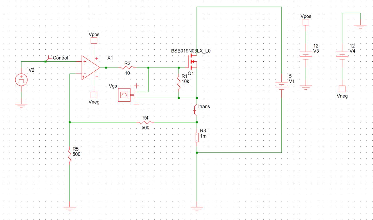
The application senriao is like below for drving power MOSFET, so I need that 2A output to drive power MOSFET, and targeting supply voltge VCC in design is ±12V.
Generally speaking, fast response and high output current are in consideration. Other spec are not so important.
Consequently, is your recommendation a combination of e.g. THS3120+ BUF634A? But sorry that I don't see BUF634A has up to 2A output capbaility, 250mA only.
Looking at the actual datasheet on the LT1210, it is more like a 1A output (min, 2A typ) -
That app note is one of many Jim wrote - I used to see him every once in a while out in the bay area where he would plug me for CFA info as he was not really a high speed guy, but a really thorough lab guy.
Anyway, that app note has too many variants in it to pursue - your specific needs will get there quicker. But -
1. Driving a power fet is all about moving the input C. That is a peak current on transition issue, not a continuous current issue - many CFA amps will put out a lot more peak than continuous (e.g., the OPA2677 will put out around 1.5A peak, but is much lower for continuous). This is rarely specified though, so hard to use that fact.
2. Need your specific circuit - but why are you asking - perhaps the LT1210 is too expensive?
Understand the points you raised. The motivation why I asked for devices to replace LT1210 is for spice-based simulation. LT1210 only has LTspice model.
BTW, I can show you what I'm trying to do as below simulation, following the basic idea of that app note, I'm using ordinary amp as X1 below instead of CFA, and I found it also works.
So it looks that power amps in TI protfilio is also a good choice.
Well thanks for the schematic, that does look like simplis,
I don't think you need the output drive of the LT part - the FET speed is pretty slow so it does not help you to drive a fast Vgs step in requiring high gate drive - also, if you reduce the gate R and gate current, higher supplies on the op amp are not necessary,
TINA V11 has that FET in the library, here is some design investigations and then the TINA file where I stopped,
Really impressed by your strong interests in this topic and all of these materials. Firstly, a little bit sorry for making you confused.
I can buy in your opinion of amp output current capability, but here I was only leveraging one FET to verify the general idea, in the actual design with the requirement of hundreds of amps of current, one FET is not enough, the gate resistor is also TBD. What's more, you're considering FET gate input as a single capacitor, but actually sometimes it is complex especially with inductive load switching, there'll be miller effect and miller current which needs continuous high output current from the driver device, to charge Cgd, making Vds drop.
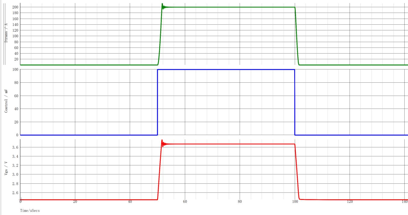
Anyway, above are not the most important contents here, I'm very interested in your feedback path design. I also find the loop seems sensitive to any one of parameters change in the circuit, showing different ringing and overshoot behavior, related to loop stability.
Several questions below:
1. At the beginning, you're just plotting the closed-loop frequency domain response, from input to output(voltage across 1m shunt resistor), to check the resonance(damping ratio), right? How did you come up with the idea to add an extra RC path from output to negative input?
2. Why you change R+C path to diode+R next?
3. Why is a bias input voltage like 10mV always there? Why not use 0V input to close the FET(make current 0A)?
1. Putting a power device inside the feedback loop adds a great deal of prop delay (phase shift) that will impair phase margin - the series RC closes the feedback loop at high F with lower phase shift holding it more stable
2. What happens to the loop when the FET cuts off? You need a feedback path for that case to keep from going open loop
3. I was just testing the FET on condition, FET off, at zero, is a tough spot for the loop to operate.
Well what Jim did might work, I am normally concerned about the loop opening up on any part of the operating range as it will have an unspecified recovery time to linear operating region - that might be fine for what you are doing, but will not be supported in any public sim model - the full internal transistor models do better but those are depending on modelling accuracy for saturated and off transistors coming back into linear region.


