This thread has been locked.

If you have a related question, please click the "Ask a related question" button in the top right corner. The newly created question will be automatically linked to this question.

DP83867CS: 10Base-Te compliance test peak difference voltage result fails

Part Number: DP83867CS
Other Parts Discussed in Thread: DP83867E

Hi Team,

When we ran a 10Base-Te Peak Differential Voltage compliance test on his DP83867CS board,
the compliance test results were as follows:
We would appreciate any advice regarding the results of the compliance test.

<10Base-Te Peak Differential Voltage Results>
1.Test Board
(1)No.1_Board
①First time  :1.55[V] ---- PASS
②second time:1.56[V] ---- PASS

(2)No.2_Board
①First time  :1.528[V] ---- FAIL
②second time:1.518[V] ---- FAIL

The above No.1_Board and No.2_Board differ only in PHY parts.

2.Procedure of test
Based on the e2e results below, we used a pseudo-random signal using the PHY BIST (0x16) function as the test signal.

<Referenced e2e>
e2e.ti.com/.../dp83867ir-10base-te-100base-tx-1000base-t-compliance-test

As the test signal, we used a pseudorandom signal generated by the PHY BIST (0x16) function.
Below, register settings
0x1f 0x8000, PHY RESET
0x00 0x0100, 10Base-T / Te mode
0x10 0x5008, Forced MDI mode
0x16 0xd80

Please tell me about the following.

[Question 1]
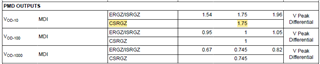
We use P83867CSRGZ as PHY component.
When I checked the description of VOD (Vpeak Differential) for 10BASE-Te in the data sheet,
I found that the MIN/MAX values for ERGZ/ISRGZ were listed, but the MIN/MAX values for CSRGZ were not listed.
Does the lack of CSRGZ specification mean that 10BASE-Te VOD (Vpeak Differential) is not guaranteed?
Please let me know if there are any regulations for the MIN and MAX values of CSRGZ.

[Question 2]
I think the output of Peak Differential Voltage varies depending on the PHY parts.
Is it possible to adjust the differential voltage output of 10BASE-Te?

Best Regards,

  • Hello,

    Could you please provide the answers to questions listed in our schematic and layout checklists? This would help establish a baseline through which we can understand if there are anything potentially contributing to this lower voltage.

    Sincerely,

    Gerome

  • Hello,Gerome

    Thank you for answering.
    Currently I'm checking the schematic and layout checklists.
    We will respond at a later date once the confirmation is complete.

    Best Regards,

  • Hello,Gerome

    I reviewed the schematic and layout checklist and added comments.
    Please check the attached documents.

    ◇schematic checklist
     SLVRBN1A_240402.xlsx

    ◇layout checklist
     SNLR048A_240402.xlsx

    Best Regards,

  • Hello,

    The Rbias combination may prove to be an issue. We would suggest an 11k with 0 ohm.

    Would removing the external CMC affect the voltage?

    What is the trace length of PHY to magnetics and also magnetics to RJ-45? What is the length of the cable being used?

    What is the impedance of the MDI?

    Can you also provide the datasheet of the magnetic?

    Sincerely,

    Gerome

  • Hello,Gerome

    Thank you for answering.
    We will answer below.

    >The Rbias combination may prove to be an issue. We would suggest an 11k with 0 ohm.
     I think it is possible to change the resistance value.
     Verify by changing the RBIAS resistor configuration from 10KΩ and 1KΩ to 11KΩ and 0Ω.
     After making the above changes, should I run the test and report the results?
     
    >Would removing the external CMC affect the voltage?
     Since we cannot easily remove all of the CMC filters, we are currently looking into ways to remove them.
     The 10BASE-Te transmission signal is the PAIRA signal (TD_P_A, TD_M_A).
     Therefore, as a confirmation method, I am thinking of deleting only the CMCs connected to TD_P_A and TD_M_A.
     Is the above understanding correct?
     Also, there is a possibility of damaging the board during modification, so I would like to check this modification last.
     First, could you please answer questions 1 and 2 in the title?

    >What is the trace length of PHY to magnetics and also magnetics to RJ-45?
    ◇Length from PHY to magnetic
     ・PAIRA(MAX) 12.3 mm
     ・PAIRB(MAX) 10.7 mm
     ・PAIRC(MAX) 16  mm
     ・PAIRD(MAX) 10.7 mm

    ◇Length from Magnetic to IX connector
     ・PAIRA(MAX) 7.1 mm
     ・PAIRB(MAX) 7.1 mm
     ・PAIRC(MAX) 8.6 mm
     ・PAIRD(MAX) 8.3 mm

    >What is the length of the cable being used?
    The cable we are using is 2.76 inches.

    >What is the impedance of the MDI?
     Differential impedance is 100±5%Ω.

    >Can you also provide the datasheet of the magnetic?
     I have attached the magnetic data sheet below.
     Also, the product name of magnetic is C26100.
     Please refer to page 2 of the attached data sheet.

    LAN transformer Catalog_C26100.pdf

    【Request matters】
    We have reviewed and attached the schematic and LAUOUT checklist.
    There was a TI FEED BACK column for the circuit diagram and LAUOUT checklist, so could you please write the answer to the question?
    Also, could you please attach the results?

    Best Regards, 

  • Hello,

    After making the above changes, should I run the test and report the results?

    Yes, please try this to see if there are any changes.

     Therefore, as a confirmation method, I am thinking of deleting only the CMCs connected to TD_P_A and TD_M_A.
     Is the above understanding correct?
     Also, there is a possibility of damaging the board during modification, so I would like to check this modification last.
     First, could you please answer questions 1 and 2 in the title?

    The specs are not guaranteed by datasheet, but we are looking at ways in which we can optimize this design to perhaps rectifying the issue.

    Removing the A pair CMC would be sufficient as your understanding is correct.


    0083.SNLR048A_240402.xlsx5873.SLVRBN1A_240402.xlsx

    Sincerely,

    Gerome

  • Hello,Gerome

    Thank you for answering.
    We will answer below.

    >The Rbias combination may prove to be an issue. We would suggest an 11k with 0 ohm.
     We confirmed the above on No.2_Board, which had the problem.
     I will report the confirmed results.
     The results showed no improvement even after changing the resistance value.
     ・1st time: 1.515V ---- NG
     ・2nd time: 1.536V ---- NG
     ・3rd time: 1.518V ---- NG

    >Would removing the external CMC affect the voltage?
    >Removing the A pair CMC would be sufficient as your understanding is correct.
     I am checking it now. We will report on this at a later date.

    >[Question 1]
    >The specs are not guaranteed by datasheet, but we are looking at ways in which we can optimize this design to perhaps rectifying the issue.
    >[Question 2]
    >I think the output of Peak Differential Voltage varies depending on the PHY parts.
    >Is it possible to adjust the differential voltage output of 10BASE-Te?
     Thank you for your answer to Question 1.
     Could you also answer Question 2?

    Best Regards, 

  • Hello,

    There is potential ways to adjust VoD however, I would like to ensure that everything else on board has been checked out before introducing this variable.

    Sincerely,

    Gerome

  • Hello, Gerome

    Thank you for answering.
    I could understand.
    Regarding your question, I will answer it next week.

    Best Regards,

  • Hello,

    I will await your input.

    Sincerely,

    Gerome

  • Hello,Gerome

    Thank you for answering.
    I was able to confirm this after removing the external filter, so I will report it below.

    Before removing the external filter, we re-ran the 10Base-Te Peak Differential Voltage Results test on the No. 2 board where the problem occurred.
    Afterwards, we conducted a test after removing the external filter.
    We will report the confirmed results below.

    1. Before removing external filter(two parts)
    (1)No.2_Board
    ①First time  :1.528[V] ---- FAIL
    ②second time:1.519[V] ---- FAIL
    ②third time  :1.506[V] ---- FAIL

    2. After removing external filter(two parts)
    (1)No.2_Board
    ①First time  :1.543[V] ---- PASS
    ②second time:1.528[V] ---- FAIL
    ②third time  :1.522[V] ---- FAIL

    After modification, there is an improvement of approximately 15 to 20 mV compared to before modification.
    However, although there were some cases where the results were PASS, most results were FAIL.

    Is there anything else I should check?

    Best Regards,

  • Hello,

    It appears that the scope has wide variation. This may cause false results. Can you please try increasing the averaging samples on the scope's compliance SW to get a more consistent measurement?

    Sincerely,

    Gerome

  • Hello,Gerome

    thank you for answering.

    >The range seems to vary considerably.
    >This can lead to erroneous results.
    >You may want to try increasing the average samples on your oscilloscope's compliance SW to get more consistent measurements.

    Please tell me about the following points.
    We investigated the parameters that can be changed during the above 10Base-Te peak differential voltage compliance test.
    However, no items were found that increased the average sample size.
    Does increasing the average number of SW samples in the oscilloscope above mean increasing the number of measurements?
    Or does it mean increasing the number of average samples taken during the 10Base-Te peak differential voltage compliance test?

    Please tell me about the following points.

    [Question 3]
    We are currently checking with equipment manufacturers to see if it is possible to increase the number of average samples for 10Base-Te peak differential voltage tests.
    If you know how to change the number of samples for the average value of the 10Base-Te peak difference voltage test, could you please let me know?
    Also, could you please attach the measurement procedure and measurement results?


    [Question 4]
    I also checked other boards, but all of them had low 10BASE-Te peak differential voltages below the average value.
    According to the data sheet, the average peak differential voltage of 10Base-Te is 1.75[V] (TYP).
    Can you tell me the compliance test results of the evaluation board for 10Base-Te Peak Differential Voltage Compliance Test [V]?
    Are you getting a result of about 1.75V(TYP)? . Could you tell me the results?


    Best Regards,

  • Hello,

    Our understanding is that upping the sampling number is able to provide more data in which the mean/true waveform is measured. In our lab, we have Tektronix scopes which are able to do this, but you will need to consult with the manufacturer of your scope if this option is available.

    Off of the DP83867RGZR EVM, we see ~1.67V when testing 10Base-Te. However, this can be attributed to differences in board design and component variation. If you are seeing consistently on the low end, this could be indicative of a design error somewhere within the MDI. 

    You may also see what happens when you place the E/I version on your board to see if that too is acting up.

    I also notice that you are writing Reg 0x16 = 0xD804. Can you try writing 0xD004 instead?

    Sincerely,

    Gerome

  • Hello,Gerome

    thank you for answering.

    >In our lab, we have Tektronix scopes which are able to do this,
    >but you will need to consult with the manufacturer of your scope if this option is available.
    I checked with the measuring instrument manufacturer to see if the oscilloscope I am currently using has the above options.
    However, the KEYSIGHT oscilloscope that we tested did not have a function to change the number of samples.

    >Off of the DP83867RGZR EVM, we see ~1.67V when testing 10Base-Te.
    I'm thinking of seeing if I can check it with a Tektronix oscilloscope as well.
    Could you please attach the procedure and test results confirmed with the above Tektronix oscilloscope?

    >Off of the DP83867RGZR EVM, we see ~1.67V when testing 10Base-Te.
    Please check the following points.
    (Question 1): Are the mounted parts of the DP83867RGZR EVM the same as the DP83867E products?
    (Question 2): Is there an individual adjustment value for the 10Base-Te differential voltage for each PHY component,
           and is it adjusted for each component?
    (Question 3): Are there any results of checking multiple DP83867RGZR EVMs?
            Also, was there no variation depending on the parts, and the output was all about 1.67 [v]?

    >You might also want to see what happens when you put the E/I version on your board and see if that works too.
    >There are potential ways to adjust VoD however,
    I will consider replacing it with the DP83867E or DP83867I product and see if I can check it.
    However, before implementing the above, please let me know the following points.
    (Question 4): You previously answered that there is a function to adjust VOD.
           Please tell me how to adjust the above VOD.

    >I also notice that you are writing Reg 0x16 = 0xD804. Can you try writing 0xD004 instead?
    Thank you for confirming.
    We will check and contact you later.

    Best Regards,

  • Hello,

    The procedure is located on the TekExpress or TDSET3 manual which is available online. 

    The voltages from the two boards measured in lab were around 1.65-1.68V. 

    To adjust VoD, we have Reg 0xA0 and 0xA1. Please note these are trim values. 

    A0[3:0] adjusts Channel A, while [11:8] adjusts Channel B.

    A1[3:0] adjusts Channel C, while [11:8] adjusts Channel D.

    Sincerely,

    Gerome

  • Hello,Gerome

    thank you for answering.

    >I also notice that you are writing Reg 0x16 = 0xD804. Can you try writing 0xD004 instead?
    I tried the above, but the result did not change.
    I also configured the MDIO register according to the 10 Base Standard in Appendix B according to How to Configure DP838xx for Ethernet Compliance (SNLA239B), and set the PHY to reverse loopback mode and confirmed it.
    Setting the PHY loopback mode did not change the results, so I think there is no problem with the test procedure.

    >(Question 1): Are the mounted parts of the DP83867RGZR EVM the same as the DP83867E products?
    I checked the evaluation board's circuit diagram and BOMLIST, but there was no detailed product name listed.
    Therefore, I would like to confirm.
    Could you please give me the answers to Questions 1?

    >To adjust VoD, we have Reg 0xA0 and 0xA1. Please note these are trim values.
    >A0[3:0] adjusts Channel A, while [11:8] adjusts Channel B.
    >A1[3:0] adjusts Channel C, while [11:8] adjusts Channel D.
    Thank you for your answer.
    I am checking about the above register.
    After checking, I would like to ask you a question.

    Best Regards,

  • Hello,

    This device would typically be the ERGZR version of the DP83867.

    Sincerely,

    Gerome

  • Hello,Gerome

    thank you for answering.

    >To adjust VoD, we have Reg 0xA0 and 0xA1. Please note these are trim values.
    >A0[3:0] adjusts Channel A, while [11:8] adjusts Channel B.
    >A1[3:0] adjusts Channel C, while [11:8] adjusts Channel D.
    We were able to confirm that changing the Channel A register above passed the 10Base-Te Peak Differential Voltage Compliance Test.
    Please tell me the following points.
    【Question 1】
    The above A0 and A1 registers exist from Channel A to Channel D.
    Are the above registers commonly used in 10, 100, and 1000BASE-T?
    Also, is there a register to adjust only 10BASE-T VOD?

    【Question 2】
    We are considering replacing it with the DP83867E product.
    We read the A0 and A1 registers, which are VOD adjustment registers, for two existing DP83867CS boards.
    Then, I checked the register values from ChannelA to ChannelD.
    When I checked, I found that the following adjustment values were included instead of fixed values.
    Therefore, I would like to confirm whether the DP83867E product has similar values.
    Can you tell me the values of ChannelD from ChannelA of DP83867RGZR EVM (DP83867E product)?

    1.Read values from A0 and A1 registers
                 A0[3:0]  A0[11:8]  A1[3:0]  A1[11:8]
    ①Board A       :    06      07     06      07
    ②Board B       :    08     07      07      05
    ③DP83867RGZR EVM :   ?     ?     ?     ?

    Best Regards,

  • Hello,

    Typically these registers are not commonly used, but in certain applications where the design has already been checked out, these have proven to have positive impact on VoD.

    As I had mentioned prior, this value is a trim value, thus the register contents may change depending on part. Thus, the PHYs on the EVM may have differing values as well.

    Sincerely,

    Gerome

  • Hello

    I think 100 and 1000BASE-T also need to be tested again by changing the values of the A0 and A1 registers.

    Therefore, could you please answer even just question 1? .

    Best Regards,

  • Hello,

    The answer is still appropriate regardless of speed.

    Sincerely,

    Gerome

  • Hello

    Are you aware that changing the A0 and A1 registers may affect 10/100/1000BASE testing?

    Please answer with YES or NO.

    Best Regards,

  • Hello,

    This register will also change VoD when in 1G, 100Mbps, and 10Mbps.

    Sincerely,
    Gerome

  • Hello, Gerome

    Thank you for answering.

    I'm closing this thread because I received the answers I needed.

    Best Regards,