FAQ: Logic and Voltage Translation > Ground-Level Translators >> Current FAQ
TXG devices (both push-pull and open-drain) cannot support any level of IEC-ESD. However, IEC-ESD can still be achieved by using a protection device like the ESDS30x product family.
The ESDS30x family can support ±30kV contact and air gap discharge. The only drawback is the DC breakdown voltage of 4.5V (min). There is a possibility these device will start to breakdown before reaching 5.5V which is the max recommended voltage condition.
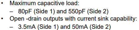
Since the I2C protocol limits the allowable bus capacitance to 400pF (for Standard and Fast Mode) or 550pF (for Fast Mode+), similar requirements will need to be implemented on the TXG8122-Q1.
There are two main factors that determine I2C bus capacitance: 1) Input cap present on SDA and SCL, 2) cable capacitance.
Input Capacitance: The input cap from SDA and SCL is 5pF (typ). This value is very minor when compared to the cable capacitance, especially you if are communicating with one device. However, the input capacitance will continue to increase as more device (or peripherals) are added to the I2C bus.
Cable Capacitance: A good rule of thumb for cable capacitance is 1pF/cm. If Standard Mode is used, the max cable length 4 meters (or 13 feet).
To support higher capacitance loading, it’s recommend to place TXG8122-Q1 Side 2 (SDA2 & SCL2) with all other I2C peripherals.
FAQ: Logic and Voltage Translation > Ground-Level Translators >> Current FAQ
At the moment TXG QFN packages do not support wettable flanks. However, we are working towards supporting wettable flank packages once products are fully released.
The QFN packages that will support wettable flanks will be RUC and DSG
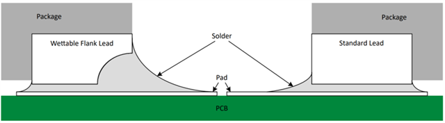
What are wettable flanks?
Wettable flanks improve side wetting after soldering which makes QFN packages easier to inspect with automatic optical inspection (AOI). A wettable flank can be dimpled or step-cut to provide additional surface area for solder adhesion which assists in reliably creating a side fillet as shown in the figure. For additional details, see the mechanical drawing.
FAQ: Logic and Voltage Translation > Ground-Level Translators >> Current FAQ
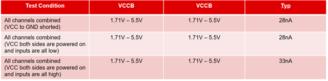
The leakage between two grounds can be found under the Electrical Characteristics section in the datasheet.
Using the TXG1041 datasheet, as an example, the leakage values are:
FAQ: Logic and Voltage Translation > Ground-Level Translators >> Current FAQ
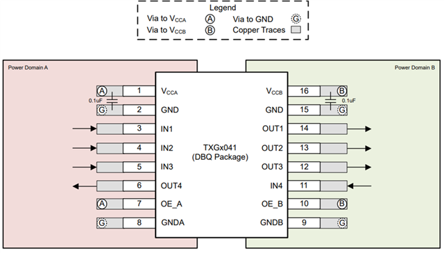
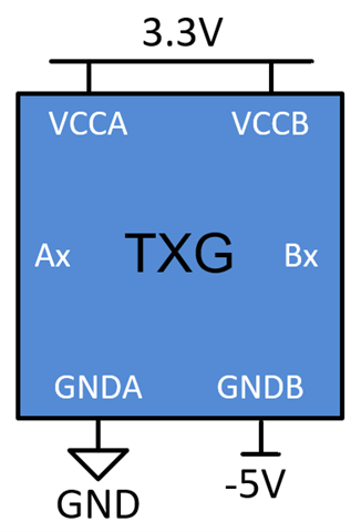
The TXG product family can be used as a regular level translator (VCCA > VCCB or VCCA < VCCB) or in a buffer configuration (VCCA = VCCB).
If a user doesn’t need ground shifting but requires a level translator with exceptional output skew and data rate parameters, they can simply tie GNDA and GNDB together.
If ground shifting is needed, we require VCCA/GNDA and VCCB/GNDB to be separated, similar to the image below.
FAQ: Logic and Voltage Translation > Ground-Level Translators >> Current FAQ
The maximum trace length that ground-level translators (as well as logic devices) can drive is 60 mm. This is a safe trace length for most devices to drive across the majority of applications. This can often be pushed to 120 mm (4700 mil), however users may see signal integrity (SI) issues between these two values.
The 60 mm standard can be shown mathematically from the typical device bandwidth, 300 MHz, and the typical effective permittivity of a PCB εr, around 4.
Users can use this excel to calculate the maximum trace length: 2313.Maximum Trace Length Formula.xlsx
For more in-depth information, see [FAQ] What is the maximum trace length that a logic device can drive?
FAQ: Logic and Voltage Translation > Ground-Level Translators >> Current FAQ
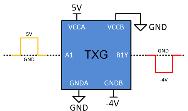
To use the ground shift capability, voltage supplies need to be separated and fall within the recommended operating conditions.
Let’s use the figure above as an example. Both supplies are connected together and GNDB shifts by -5V due to parasitics in a long wire. While A-side is fine, B-side exceeds the supply-ground absolute maximum ratings. To avoid similar scenarios, it’s recommended to kept both supplies (and their respected ground) separated.
FAQ: Logic and Voltage Translation > Ground-Level Translators >> Current FAQ
A negative signal can be generated from ground-level translators as long as the user’s system has a negative supply rail. To prevent damage to the IC, the difference between VCC and GND needs to fall within the recommended operating conditions.
Let's use the image below as an example. VCC and GND for both A-port and B-port fall within the recommended conditions. The output signal will toggle between VCCB and GNDB which in this case is 0V and -4V.
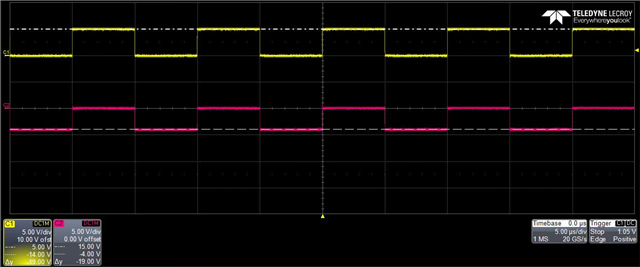
Using the same test conditions on the TXG8041, the output waveform (pink) toggles between GND and -4V.
FAQ: Logic and Voltage Translation > > Current FAQ
FAQ: Logic and Voltage Translation > Ground-Level Translators >> Current FAQ
| Ground-Level Translators | Digital Isolators | |
| GNDA to GNDB Difference | 80V | 3kVrms |
| Galvanic Barrier | No | Yes |
| GNDA to GNDB Leakage (VCC to GND Shorted) |
70nA | <1nA |
| Size (4-Channel) | 4mm² | 29.4mm² |
| Propagation Delay (3.3V) | 5.8ns | 18.5ns |
| Ch-Ch Skew (3.3V) | 0.35ns | 4.7ns |
| Data Rate | >250Mbps | 100Mbps |
| Level Shifting Capability | 1.71V to 5.5V | 1.71V to 1.89V and 2.25V to 5.5V |
| Operating Temperature | -40ºC to 125°C | -40°C to 125°C |
| CMTI | 1kV/μs | 100kV/μs |
| Certifications (UL, VDE, Surge) | No | Yes |
| EMC (EFT, RI, IEC-ESD) | No | Yes |
More information on Ground-Level Translators can be found here (link)
