This thread has been locked.

If you have a related question, please click the "Ask a related question" button in the top right corner. The newly created question will be automatically linked to this question.

LM51561: Converter not starting from power up suspect due to encountering current limiting

Part Number: LM51561
Other Parts Discussed in Thread: TL431, LM5156

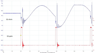
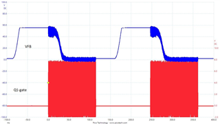
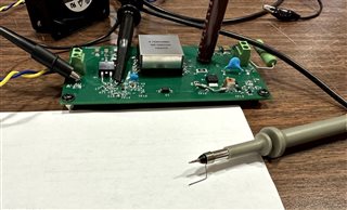
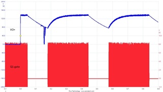
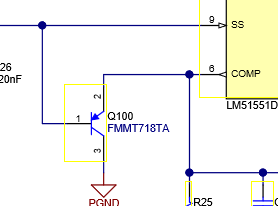
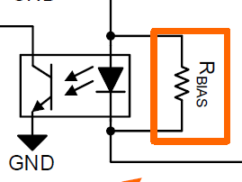
Hello, I am prototyping a 50V to 150V DC flyback converter design. First article of the prototype has been assembled but it is not starting up. I believe the converter is encountering over-current and after the 64 tries during startup, it resets. The controller tries again repeatedly. I have tried various changes as shown by the redline changes in the schematic. I have captured and attached the important waveforms also. 

FYI, I also tried changing to 400kHz switching from 250kHz by replacing RT and this resulted in Q1 N-channel FET and T1 failure after a few seconds and the FET getting very hot. I have since replaced the Q1 and T1, and the prototype is back to behaving as previously, i.e. continuously resetting. Please provide your suggestions and remedies. 

Kind regards, Denny Wong

Ikomed Technologies

dennyw@ikomed.com

www.ikomed.com

20231016_Ikomed_lm51561.zip

  • Hello Denny,

    You are right, this looks like hiccup mode. There is a lot of noise on all the signals. is this because you use a long GND connection on the oscilloscope probe or are you already using a very short GND connection?

    Please check  this article: How to measure ripple for better design outcomes - Power management - Technical articles - TI E2E support forums

    Would it be possible for you to check the schematic by using our quickstart calculator for flybacks? SNVC240 Calculation tool | TI.com

    Best regards,
    Brigitte

  • Hi Brigitte,

    Thank you for your assistance. I believe the noise is ground bounce when Q1 switches off. The bottom side contains a split plane of primary ground and isolated-secondary grounds. The ground test point is SMD and has to via to the bottom side.

    The TI calculator was useful, thank you. It's better than one I derived from the datasheet formulas.

    I've captured and attached new waveforms after adding RSL and changing RS back to 15mOhm. The voltage at RS when Q1 is enabled is between 0.8V and 0.5V. This translates to instantaneous currents of 54A to 33A. If this is real, it explains why the controller is in over-current. I've added RSL and it modified the circuit's behavior but continues to go into over-current.

    Question: what should be the nominal voltage at the opto-isolator primary side collector be? How should the pull-up be sized?

    Based on the converter's functional block diagram in data sheet page 12, hiccup mode is associated with VCS1 (I-slope) only, and not VCS2. Is it clear to you that the converter is going into hiccup mode? Is it possible the controller is detecting over-current due to the secondary feedback at COMP pin because the pull-up is not sized properly?

    Viewing the Q1-drain waveform, the drain voltage is at 3 different levels (~30V, ~20V, and ~40V) for three consecutive cycles when Q1 is enabled. Why is Q1 not saturating? Should I have used a N-ch MOSFET with lower Vgs?

    Any other suggestions you can offer? Thank you.

    Kind regards,

    Denny

    Ikomed Technologies

    dennyw@ikomed.com20231021_150vdc_ps.zip150vdc_isolated_ps_redline.pdf4520.LM5155_56_Excel_Quickstart_Calculator_for_Flyback_Regulator_Design.xlsx

  • Hello Denny,

    Please give us another day to review your data and come back to you.

    Best regards,
    Brigitte

  • Hi Denny,

    The drain voltage is very strange. Can you check if there are damaged components? Can you also check the input voltage?

    Can you check if TL431 is damaged as it can survive 36V max.

    Best Regards,

    Feng Ji

  • Hello Feng Ji and Brigitte,

    Thank you for continuing to provide support. I believe both devices are still functioning. The evidence is as follows. I have since gotten the p/s to start-up when unloaded, but does not start-up still even when lightly loaded. When the p/s has started, the waveforms appears to indicate the devices are functioning, Q1 is conducting current as seen by voltage across RS. TL431 cathode reaches 2.495V nominal.

    Related to TL431, I had the same suspicion when I first saw the waveform. I believe the cathode is rising to the voltage potential shown but no current is flowing. Since VO+ has not reached its designed nominal level (i.e. 150V), therefore, TL431's REF pin is not at the 2.495V nominal level also and the TL431 device is acting in a transient state.

    I have since gotten the p/s to start-up when output is unloaded. The change that got the p/s to occasionally startup was replacing the opto-isolator R-pull-up (R5) to 2k67 ohms. The change that got the p/s to consistently startup when unloaded is re-connecting the secondary soft start circuit, i.e. Schottky diode D6. I also replaced the secondary soft start timing resistor R18 to 976K ohms to improve the start-up time. Interestingly, when I replaced R18 with 396K ohm, the circuit had startup issues again.

    It appears the startup mechanism is the controller charges the output capacitor level but maintains a low duty cycle due to sensing over-current. The output charges but the controller stops after its fixed number of operating cycles. The output capacitor begins discharging. The controller begins another startup cycle and charges the output capacitor again, but will stop again. The average output level climbs incrementally and if it reaches the operating level of 150V, then the controller is able to begin normal operation.

    When the p/s is loaded with 22mA resistive load, the p/s does NOT startup. In this case, the load discharges the output capacitor during the controller's retry off state and the output climbs to a quasi steady state of charging and discharging the output capacitor. If the output level does not reach 150V, the controller and p/s remains in this quasi steady state.

    I am guessing the description I provided is not how TI intended the controller to start up.

    I have improved the grounding of RS as seen in the attached RS waveform. The sense voltage is now ~0.4V or 26.7A peak (versus ~0.8V peak previously) and may possibly be real. I don't think I can improve the grounding further without a re-layout of the PCB. Even then, I believe it will be incremental. 

    Questions:
    1. Is the waveform at the controller's COMP pin (net FB_COMP), now reasonable?
    2. The waveform at the TL431 cathode (net VFB) does not appear normal. Any thoughts?
    3. The drain voltage is still showing Q1 does not saturate. Thoughts?
    4. Any ideas how to increase the duty cycle so the output capacitor charges faster and to a higher level?
    5. Increasing the operating frequency to 400kHz caused Q1 and T1 to fail previously. However, the circuit and component values were not correct previously also. Will changing the operating frequency now help?

    Your help is greatly appreciated. Thank you.

    Regards,
    Denny

    20231025_150VDCps_unloaded.zip20231024_150VDCps_22mALoad.zip0572.150vdc_isolated_ps_redline.pdf

  • Hello Denny,

    Can you please try to increase the softstart time by incrreasing both capacitors C8 and C14?

    For the bigger pullup rresistor you are using now, i think the LED resistor R6 is too big. Please try to decrease this value also.

    The compensation of an isolated flyback is normally done on the secondary side only, so please remove C9 and R17 for the next test. It is possible that there are components needed but not necessarely of the same value the compensation uses.

    And can you measure the voltage at the CS pin directly please?

    Best regards,

    Moritz

  • Hi Moritz el al,

    Thank you for your suggestions. Attached waveforms have both soft start capacitors increased.

    I decreased the LED biasing resistor to 35k and now the p/s starts up with a 6k8 (~20mA) resistive load but only to 139V output voltage. The waveform at TL431 cathode is very odd. I replaced it (D4) but the waveform did not change.

    I captured the waveform at CS pin as requested.

    Any suggestion is appreciated. Thank you.

    Regards,

    Denny

    20231027_Ikomed_150Vps.zip2330.150vdc_isolated_ps_redline.pdf

  • Hi Denny,

    The voltage at D4 cathode is way too high. Abs max is 37V and in your scopeshots it is nearly 60V.

    The input voltage for the optocoupler needs to be clamped by a zener diode in case of high output voltages.

    As an example please have a look at this reference design: https://www.ti.com/tool/PMP10712

    The resistor and capacitor values for this case can be calculated using the powerstage designer: https://www.ti.com/tool/POWERSTAGE-DESIGNER

    Under control loop, there is the option to choose Type 2 compensation with zener diode.

    Best regards,

    Moritz

  • Hi Moritz et al,

    I've added the zener circuit as suggested. Note the p/s is no longer starting up and is in a repeating retry state.

    I set the zener bias to 4.5mA nominal (29k5 pull-up) for VO+=150V. However, the p/s output only reaches to ~100V average so the zener bias current is actually ~2.8mA average instead.

    The LED bias current is 2.5mA from the 18.2V zener voltage and 5k62 bias resistor. This should be enough bias current for the TL431 to operate. The TL431 REF pin does not see 2.495V as VO+ is not rising to 150V. I am not sure how the TL431 cathode behaves when its REF pin is below its Vref threshold voltage. Viewing the waveforms at VFB and at the LED-anode, it appears the opto LED is forward biased. However, I am not sure the TL431 cathode is behaving properly.

    The opto's collect continue to appear to be high at ~3V average. I increased the pull-up to 5k11 from 2k67 which should lower the operating point at the collector. But the average level remained the same at ~3V.

    Due to the p/s not working, and the TL431 may have been over-stressed, I replaced the TL431 again but the waveforms did not change. I replaced the opto TCMT1107) also again without changes to the waveforms.

    Interestingly, the voltage on the CS pin indicates the device is no longer in over-current, peaking less than 50mV. However, the converter duty cycle continue to be very low duty cycle. Q1 drain appears to get to saturation but only during a portion of the on-time.

    Viewing VO+ again, the controller stops charging the output capacitor to a higher level even though it has not finished all the number of cycles before resetting and retrying. Like it thinks the output level has reached what it thinks it is supposed to be already.

    I used a short ground on the scope probe to capture the latest waveforms as shown in the attached photo.

    Please provide further suggestions if you have any.

    Kind regards,

    Denny

    150vdc_isolated_ps_redline_20231101.pdf20231101_150VDC_ps.zip

  • Hi again,

    I attached additional waveform to further supplement the suggestion that the converter stops charging the output capacitor to a higher required level. 

    Denny

  • Hi Denny,

    The signal at COMP is now at the max. value. This means a high duty cycle is requested. The fact that there is nevertheless only a very low duty cycle means that there is an overcurrent condition happening. Also in the picture you send last, the time where the switching stops matches with the 32768 hiccup cycles.  Hiccup will only happen in an overcurrent condition.

    The waveforms at CS pin and PRI_CS does not match together. PRI_CS shows a voltage of around 300mV, CS only 50mV. There has to be something wrong.

    The waveform at Q1 drain also looks very strange becuase the voltage goes down before switching.

    Can you please try to exchange the LM51561 and also the MOSFET?

    And can you also please send the layout?

    Best regards,

    Moritz

  • Hi Moritz,

    Attached waveforms are with LM51561 and N-channel MOSFET replaced. The output is not starting up and only reaching to ~30V. The waveform at CS pin is interestingly indicating over-current.

    I've attached the PCB CAM files and png files of some of the layers in case you don't have a Gerber viewer handy.

    I have made a modification to the primary ground connection of the current sense resistor R14. I drilled a 1 mm hole adjacent to the pad and connected a solid wire from the pad to the primary ground plane on the bottom side. This modification reduced the voltage at PRI_CS node by half (~0.8V to ~0.4V peak).

    The waveforms were captured with a 5k6 resistive load (20mA). I removed the load so the p/s is unloaded. The output did not have the discharge droop but still did not rise to intended output voltage.

    I am thinking of reducing R14 from 15 mOhm to 7.5 mOhm again which should allow a higher transformer primary current. I intend to try this tomorrow.

    Please let me know if you have any suggestions. Thank you for your help.

    Regards,

    Denny

    20231102_Ikomed_150VDCps.zip150vdc_isolated_ps_CAM.zip20231102_CAM_png.zip

  • Hi Denny,

    Yes you can try to decrease the current sense resistor again, but this seems to be a problem related to the layout.

    We recommend to follow the layout guidelines given in the datasheet of the device. You can also have a look at the layout of the LM5156 flyback EVM: https://www.ti.com/lit/ug/snvu736/snvu736.pdf?ts=1698999757445&ref_url=https%253A%252F%252Fwww.ti.com%252Ftool%252FLM5156HEVM-FLY

    The ground connection of the current sense resistor and the IC has to be very close together. Even with the hole drilled, it is a long distance because of the tracks interupting the GND plane. Also the switching signal loop for example is very large.

    Best regards,

    Moritz

  • Hi Denny,

    What you should also do is to connect a PNP transistor to COMP and SS like shown below:

    Otherwise the primary softstart capacitor has no influence.

    Also a bias resistor for the opto LED should be implemented:

    Best regards,

    Moritz

  • Hi Moritz,

    Good news. The p/s is now starting under load. Adding the PNP transistor as you recommended made the difference. I first tested the change unloaded. Then tested with 22mA load. Finally with 44mA load. The output startup waveform is similar under the different load conditions. The p/s starts up consistently. I will continue with more testing in the following days. 

    I did not add the Rbias across the opto-isolator LED. I wasn't sure how to select the value and think it may take some iterations. 

    Revised waveforms and schematic are attached. Any comments about the waveforms would be useful. Level at CS pin is negative when the FET gate is driven. The scope ground was placed on the more negative terminal of the sense resistor R14. Likely there is still offsets exist in spite of the modifications I made. 

    Thank you for your help and recommendations. 

    Kind regards,

    Denny Wong

    20231106_Ikomed_ps.zip3806.150vdc_isolated_ps_redline.pdf