UCC28951: Transformer heating shoot up gradually

Part Number: UCC28951
Other Parts Discussed in Thread: PMP6712, TL431

Tool/software:

Dear TI Team,

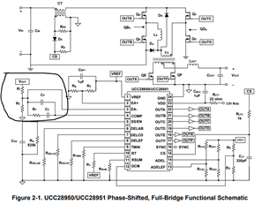
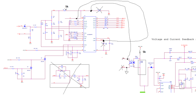
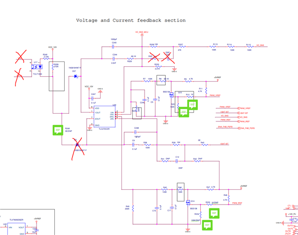
I have implemented PSFB DC-DC,3.3KW input is 400V DC, output is 420V,DC.8A for charging appilcation

I have got output and all,but transformer heat is not stable,it keeps on increasing and went to 90deg still increasing

what could be the reason for this 

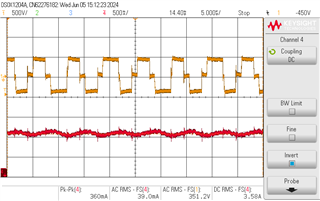
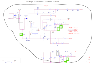
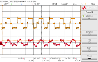
Attached Transormer Voltage and current,for output 4A Rheostat load

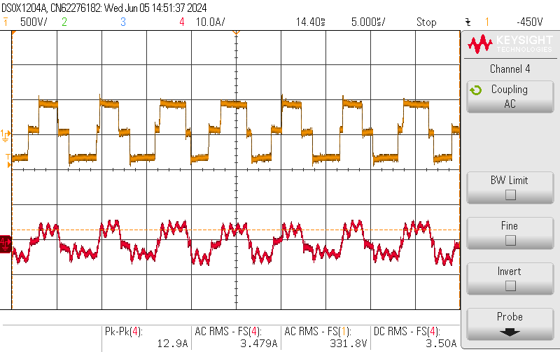
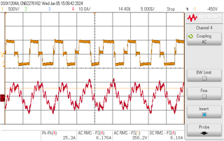
below is for 8A Rheostat load

let me know reason for transformer heating,Rsum pin is connected via resistor to Gnd to ensure Peak current mode to avoid DC at transformer

Thank you

  • I enquired and ensured magnetic vendor to limit copper losses,core losses,skin and proximity loss to be very less

    Even i tried with lower current say 4A also temperature is not stable and keep increasing gradually

  • Hello,

    I am reviewing your inquiry and will get back to you shortly.

    Regards,

  • Hello,

    Your transformer current does not look typical it also has lots of ringing on it.  Your rheostat is a wire wound inductor.  This inductance may be causing the excessive inductor ringing that you are seeing on the primary.  Try using a resistive load or electronic load to see if you can remove it.

    When it comes to transformer heating, there is core loss and copper loss.  If your peak current and RMS current is what you told the magnetic designer it should be the magnetic should not be getting hot.  You also need to make sure it was designed for the ambient temperature where the design is being used.

    I would double check the RMS current and the peak current in the transformer to make sure it is what you told the magnetic designer. If it is then then the transformer was designed incorrectly.  If it is not then gave the magnetic design the wrong specifications and need to give the designer the correct specifications.

    Regards,

  • Hi thanks,

    Below is the Primary switch Voltage and Load current,same rheostat load,i think rheostat load may not be causing,confirm me

    I Will check with electronic load as well

    Thank you

  • Venkatesh,

    It is hard to pin point the root cause with limited information. What is the expected transformer temperature? Based on your simulation? At 8A output for 420V DC, that's 2.2kW. Even 0.1% power loss on transformer is 2.2W. Have you run any thermal simulation?

    Have you checked the control waveform to ensure it works properly?

    Best,

    Ning

  • dear sir,

    i wasnot done any thermal simulation

    help me to design thermal constraint,i have tried adding Heatsink to transformer also

    Thank you

    venkatesh B

  • Venkatesh,

    Again, without much details, like schematic and other waveforms, it is hard to give you any specific guidance. I suggest you to contact our local sales team to get some help from our PDS team for system level design.

    Best,

    Ning

  • Good morning,Ning Tan

    I herewith attached schematics of PFC and PSFB

    Let me know waveforms would like to check,i will share that


    3.3KW_PFC_PSFB.pdf

    Thank you

    venkatesh B

  • Venkatesh,

    It will take us some time to review the schematic. We will get back to you soon.

    Ning

  • Hello,

    I reviewed the schematic and the UCC28951 controller and surrounding components seems to be missing. Can you share that schematic as well with feedback compensation?

    Regards,

  • Hi mike O,

    Thanks for review.

    I herewith attached complete schematics of PFC,PSFB and controller schematics

    Kindly do review and share your valuable points please

    controller.pdf

    psfb_updated.pdf

    4024.power.pdf

    Thank you

    venkatesh B

  • Hello,

    Your information has been received and is under review.  I will get back to you shortly.

    Regards,

  • Hello,

    I reviewed your 4024.power schematic which is the power stage for the PSFB.  With an output power of 3.3 kW I don't believe 68 uF of output capacitance is enough.  You might want to check the size of the output capacitor bank.  The following link will bring you to an application note (slua560) goes through the step by step design process of a phase shifted full bridge (FSFB).  There is a section on sizing the output capacitor based on loading and hold up time.  You can use this to check and size your output capacitor.

    https://www.ti.com/lit/pdf/slua560

    I reviewed psfb_updated and it looks like you are tying to use an adaptive delay approach.  This is being done by the resistor dividers off the current sense pin to ADEL and ADELEF.   I would recommend using a fixed delay approach because it easier to setup the timing.  How to use this approach is covered in application note SLUA560.

    You had mentioned that the design is stable and the only issue is transformer heating.  When I look at the transformer primary voltage vs load current.  The duty cycle seems to be changing every switching cycle.  This is not normal and the feedback loops should not be correcting every switching cycle. In peak current mode control designs and using an opto isolator it is recommended to cross the voltage and current loops to less then 5 kHz.  You might want to double check and reset your compensation to increase phase margin and gain margin.  Typical loops cross over at 2 to 3 kHz.

    To prevent a transformer from saturating you need to maintain volt second balance across it.  Since the input voltage of the transformer shows varying duty cycle every switching cycle, the transformer might be partially saturating leading to heating of the transformer.  I would work on stabilizing the feedback loops to get the duty cycle to be more constant.  This should help reduce partial transformer saturation and heating in the transformer.

    Regards,

  • Hi mike

    Thank you for your response,i am completely agree

    could you please help me to fine tune this loop please 

    thank you

  • Dear sir,

    I herewith attached updated PSFB controller schematic, yes i am not using adaptive delay approach

    i have taken compensation values from design excel sheet except i connected a Resistor R58 to 10K(value identified in another reference circuit in TI) to operate converter in CCM mode.

    Kindly advice me circuit element to play with please

    psfb_updated_2.pdf

    I am waiting for your reply

    Thank you

    venkatesh B

  • Hello,

    R15 and R21 are still populated on your schematic.  So this design will still try to operate in adaptive delay.   You need to unpopulated these resistors to have a fixed delay approach.

    This compensation in the excel is not the same as what your design is using.  The excel tool is based on the following application note and uses the on board amplifier and used for secondary side control.  I have circled the circuitry for your reference.

    https://www.ti.com/lit/pdf/slua560

    Your feedback is different than what is used in the application note and excel tool. 

    I have circled your feedback components from your schematics this looks like you are trying to do constant current voltage mode control.

    Did you copy a TI reference design and if so could you tell me which one?  The feedback on the controller side of the schematic does not look correct for opto feedback. 

    Regards,

  • Dear Mike,

    I am using PMP6712,1.6KW Reference design,infact i merged Cp,Rf,Cz with 10K from reference design

    i understood now this is not a good method,help me arrive at proper values of compensation please

    meantime i will try removing ADEL by DNP R51 & R21

    Thank you

  • Hello,

    Your inquiry is under review and I will get back to you shortly.

    Regards,

  • Hello,

    Your compensation scheme looks different than PMP6712.  The PMP6712 seems to be using to PSFB in parallel/interleaved.  Your design is different only using a single phase.  

    I reviewed the compensation scheme used in PMP6712 and I don't believe the opto transistor is connected correctly (Opto E).   The opto  transistor should be ground referenced.

    The following schematic shows the proper connections of the opto transistor and TL431 feedback for voltage.   Please note the opto transistor is ground referenced.

    If you are trying to do constant current constant voltage mode control.  The following link will bring you to a 2 kW battery charger reference design that shows a feedback scheme that will work for this application.

    https://www.ti.com/tool/PMP8740#tech-docs


    Regards,

  • Hi mike,

    Thanks,

    In 2KW reference charger(controller IC ground & secondary ground is same), they have not used OPTO feedback, directly feeding from opamp to Ea-

    since we are using opto and giving to Ea+ because of different ground potential.

    In reference designs, those using OPTO giving to Ea+, Ea- for not using Optos

    In Excel calculation tool also give compensation for without OPTO only

    Kindly help me to address the current issue,i have no idea about doing this,since board is fabricated,assembled so difficult to change entire circuit

    U can suggest me connection so that i will do that please

    Thank you

    venkatesh B

  • Hello,

    Your inquiry is under review and I will get back to you shortly.

    Regards,

  • Hello,

    Your circuit is different than any other voltage control, current loop that I have worked on.  Also, the UCC28951 was designed for secondary side control. So there is no application note that I can send you to compensate both loops.  Other customers have gotten the UCC28951 to work with opto isolator feedback, so you should be able too.  I believe your opto coupler is set up incorrectly.  I marked up the schematic showing how the connections should be setup.  This feedback is similar to one previously referenced.

    If you remove diode D3 in your feedback circuitry you will only have the voltage loop feedback.  If we assume the opto has a CTR of 1, you can use the excel to compensate the voltage loop.  So you don't run into issues with the opto pole, which generally occurs at 5 to 10 kHz, I would recommend crossing the voltage loop over at 2 kHz.  I would then double check the feedback loop with a network analyzer.  

    The following link will bring you to an application note that discusses how to design a PSFB using the UCC28951.  There is a section on compensating the voltage loop in the application note.  The excel tool uses the same equations that are in the excel design tool.  Please make sure you add the correct amount of slope compensation to avoid sub harmonic oscillations in your design.  Setting up the slope compensation is covered in the application note and there are calculations for doing it in the excel design tool.

    https://www.ti.com/lit/pdf/slua560

    I would recommend compensating the voltage loop and testing it before trying to compensate the current loop.

    I reviewed your feedback for the current loop and it looks similar to the 2 kW design, I refenced previously.  I believe it will work with the corrected opto coupler feedback as well.  However, you will have to debug it and compensate this loop.  When you do cross over the current loop, you might want to cross it over at 1 kHz, so it does not fight the voltage loop.

    Regards,

  • Hi mike,

    Good morning,

    I will do it today and let you know if i got stuck

    Thank you so much

  • Hello,

    Thanks for letting me know.

    Regards,

  • Hi mike,

    I had tried the changes and started testing the Voltage control section alone.

    Output voltage set point is 418V,but it is not controllable going beyond 418V,reached 440V and above,we turned off when it reaches 440V still it keeps on increasing

    I tried connecting load as well there was no current control either

    what could be the reason for this 

    Thank you

  • Hello,

    Could you send me updated schematic for review?

    Regards,