Hi TI Experts,
I have the below queries regarding the VPP supply selection, configuration and application connected to the VPP pin of the SoC.
- When is VPP required
- Difference between GP and HS-FS hardware boards
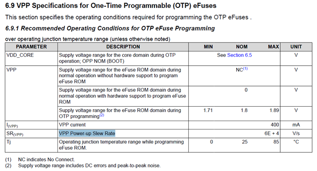
- What are the VPP voltage and current specs?
- What is the recommended VPP supply solution?
- Can I use a load switch or FET to switch the supply?
- LDO specs to consider.
- Should i use a dedicated supply?
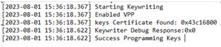
- Steps for eFuse programming
- How should I terminate the VPP supply pin for GP devices with no HS-FS provision?
- How should I terminate the VPP supply pin for HS-FS device used as a GP device?
- How should I terminate the VPP supply for HS-FS devices when not programming the eFuse
- Any suggestion for reducing OTP write failure.
- Do you have any additional recommendations?
- Does the above guidelines apply for AM64x, AM62A7, AM62A3, AM62P and AM62Px devices?
- On the SK TLV75518PDQNR is used. Is there an LDO recommendation for automotive applications?
Let me know your thoughts.