


Other Parts Discussed in Thread: FDC2214, TPS65133, BUF634A
Dear TI experts,
In my application, the BUF602 acts as a voltage buffer for active shielding of the FDC2214 capacitance-to-digital converter.
For active shielding, the signal on the LC tank circuit of the FDC2214 system should be the input.
The signal is a half-sine wave with a typical amplitude of 0 to 1.8V and a maximum frequency of 10MHz.
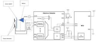
Ideally, the phase shift and amplitude difference between the input and output should be minimized.
Here I have three questions about setting up the BUF602 in my application.
1.
Since the FDC2214 has 4 channels, 4 BUF602 chips need to work on the same PCB.
Does each BUF602 need a separate decoupling capacitor?
The ±5V will be provided by the TPS65133 split rail regulator, and the trace between the TPS65133 and the BUF602 is about 3-4cm.
There will also be about 2cm of space between each BUF602.
2.
The second problem is the middle reference pin setting.
I'm not sure if this pin is useful for my application.
If I don't use this pin, should I leave it floating?
3.
In my application, the BUF602 needs to drive a load capacitance of about 330pF.
This capacitor is actually made up of two layers of copper in the PCB, so by increasing the thickness of insulating layer the capacitance can be reduced to around 40pF.
And it is expected that in practical applications, this capacitance may fluctuate by a few pF every 2 to 3 seconds.
According to BUF602, the input impedance is 1MΩ and the output impedance is 1.4Ω.
Do I need to introduce some external passive components at the input and output pins to maintain the stability of the BUF602 output signal?
Best regards,
Will
