This thread has been locked.
If you have a related question, please click the "Ask a related question" button in the top right corner. The newly created question will be automatically linked to this question.
Tool/software:
Our team found failure more than 50% at ICT. After checked the differences between passed and failed board and found difference at this part number TL074CDR.
Kindly help to check with supplier. We observed different marking on the component body between the pass and fail components. We need TI to please advise on the difference/ changes between these 2 IC’s. Please treat this as urgent case as we are having high failures and possible shipment delinquency if not resolved at the soonest.
![]() |
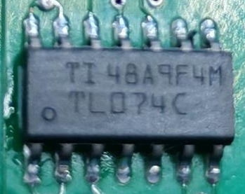
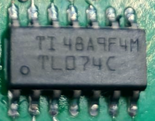
Body marking on passed board |
![]() |
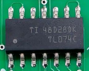
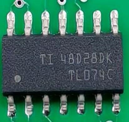
Body marking on failed board |
Incoming history:
Item |
Manufacturing Part # |
Supplier |
Packing Size |
Receipt Number |
Order Number |
Receiving Date |
Date Code |
AGIH-VR-1826-1622 |
TL074CDR |
SP7U1436X |
1250 |
WR6276888 |
70GL17208 |
10/9/2024 10:14 |
2433 |
AGIH-VR-1826-1622 |
TL074CDR |
SP7U1436X |
1250 |
WR6276888 |
70GL17208 |
10/9/2024 10:14 |
2433 |
Both markings look OK (the TL072 is made at multiple assembly sites).
Independently from the marking, a new die was introduced; see PCN# 20221219006.1. The guaranteed datasheet limits have not changed, but it is possible that your test relies on characteristics beyond these limits. Please specify exactly what test conditions you're using and what the pass/fail criteria is. (One obvious change is that the new die supports a wider output voltage range; if this is your test problem, just increase the limits.)
Mohd,
I agree with Clemens comments about the marking looking ok as well as the PCN. Additionally, I will point out the TI Anti-counterfeit policy. The key point of this policy is that the devices need to be purchased from an authorized distributors. Assuming you purchase through an authorized distributor, you should not have a concern regarding counterfeit devices. If you provide more detail on the specific issue (failure) you are having we can take a closer look in try to identify the problem.
Best regards, Art
Hi, above file I share you the failure occur at our site and our analysis for this issue.
The failure we got at in circuit test is at analog test. The readings obtained is around 0.98~1.4 V. While the upper limit is 5.88V and lower limit is 5.32V.
This failure is more than 75% drift from our initial test setup. We cannot afford to widen the limit as the limit reading is too wide from the original. Please also specify the output
voltage range that you mentioned wider than initial part.
Are U14 and U15 actually powered? I'd guess they are not, and the new clamping diodes from the input pins to V+ clamp the Lx_MONITOR signals.
The LM324B would have overvoltage-tolerant inputs.
Mohd,
The device was updated with a die that includes ESD protection diodes on the input and output. The old die did not have these. See image below of the new arrangement. It isn't clear to me how your test is done, but I think the addition of the ESD diodes is likely the difference. This change should not impact normal operation of the device so I think Clemens is correct and perhaps you are doing an unpowered test. If the test does have power applied, please specify the input signal and supply voltages.
best regards, Art
Yes, we do unpowered test here. But the part itself has different reading when measured raw part between leads compared to good part.
Are these differences caused by the die?
Good Raw Part Measurement (OLD) |
Bad Raw Part Measurement (NEW) |
||
|
|
||
Pin 1 to 11(-15v) |
1.400v |
Pin 1 to 11(-15v) |
0.813v |
Pin 2 to 11(-15v) |
0.672v |
Pin 2 to 11(-15v) |
0.850v |
Pin 3 to 11(-15v) |
0.673v |
Pin 3 to 11(-15v) |
0.849v |
Pin 4 to 11(-15v) |
0.579v |
Pin 4 to 11(-15v) |
0.678v |
Pin 5 to 11(-15v) |
0.673v |
Pin 5 to 11(-15v) |
0.849v |
Pin 6 to 11(-15v) |
0.671v |
Pin 6 to 11(-15v) |
0.849v |
Pin 7 to 11(-15v) |
1.401v |
Pin 7 to 11(-15v) |
0.813v |
Pin 8 to 11(-15v) |
1.404v |
Pin 8 to 11(-15v) |
0.813v |
Pin 9 to 11(-15v) |
0.671v |
Pin 9 to 11(-15v) |
0.804v |
Pin 10 to 11(-15v) |
0.673v |
Pin 10 to 11(-15v) |
0.848v |
Pin 11(-15v) |
GND -15v |
Pin 11(-15v) |
GND -15v |
Pin 12 to 11(-15v) |
0.674v |
Pin 12 to 11(-15v) |
0.849v |
Pin 13 to 11(-15v) |
0.672v |
Pin 13 to 11(-15v) |
0.849v |
Pin 14 to 11(-15v) |
1.403v |
Pin 14 to 11(-15v) |
0.813v |
One of the failures occurred is at CR49 (refer circuit below). The testing will measure the reading at node L1_Monitor (connected to TL074CDR) to ACOM.
For this test, our nominal value should be around 5.6V. However using the new part, we get around 1.4V which shows 75% drift in reading compared to the original nominal.
Are these differences also caused by the die?
Mohd,
Sorry for the difficulty you are having and I hope we can resolve them soon.
Best regards, Art
You did not mention any failures during actual operation. If only the ICT fails, then you just need to change the test limits.