This thread has been locked.

If you have a related question, please click the "Ask a related question" button in the top right corner. The newly created question will be automatically linked to this question.

DAC39J82EVM: Images, Bitstreams or Applications targeting DAC39J82EVM and Xilinx FPGA EVMs

Part Number: DAC39J82EVM
Other Parts Discussed in Thread: DAC38J84EVM

Hi,

We will be using DAC39J82EVM and ZCU106 EVM from Xilinx to Evaluate and test our Firmware, the connections are made as mentioned in e2e.ti.com/.../dac39j82evm-support-for-xilinx-zynq-ultrascale-plus-evm-zcu106.

  1. In order to check the sanity of the Received DAC EVM and to Evaluate it straight away, do you have any FPGA Images (Bitstreams) and SW tool/applications targetting Xilinx Eval boards like KC705 and DAC39J82EVM? This would really help us in Evaluating the DAC EVM Board straight away.

  2. In few forum posts, saw "TSW14J10EVM" used along with FPGA and DAC EVMs, What's the purpose TSW14J10EVM? Do we really need this board in our case for connecting ZCU106/KC705 to DAC39J82EVM? Can't we connect ZCU106/KC705 to DAC39J82EVM directly?

Please provide your suggestions.

Thanks,
Kiran

  • Kiran,

    For #1, you can do a quick verification with the KC705 if you have the TSW14J10EVM. This will allow you to operate the TI HSDC Pro software and provide working firmware. See attached TSW14J10EVM User's Guide for more info regarding this setup.

    For #2, The TSW14J10EVM is only needed if you want to run the TI HSDC Pro software. Otherwise it is not needed. This board also comes in handy when using a DAC EVM with any Zynq platform as Xilinx did not route the SYNC signal to the FMC connector. The TSW14J10EVM allows the user to use alternative pins that are route on the Zynq development kits. We also have an example of the DAC38J84EVM connected directly to a KCU105.

    Regards,

    Jim

    1104.SLAU580B.pdf1050.DAC38J84_442_122.88.pptx1033.KCU105 HSDC Pro User's Guide.pdf

  • Hi Jim,

    Thanks for the reply.

    I will go through the attached documents.

    1. Further Adding on to previous queries, Can we connect ZCU106/KC705 to DAC39J82EVM directly? Considering Syncs (in case of ZCU106) in LVCMOS logic levels as mentioned in our other post.
    2. What I understand is, for using HSDC Pro software we require TSW14J10EVM, suppose if we don't use HSDC Pro software & TSW14J10EVM, can you please point us to the tool to be used for configuring LMK on DAC EVM? Do you have any KC705 Bitstream in order to Evaluate DAC EVM along with the tool configuration file for LMK ?

    Please provide your feedback.

    Thanks,

    Kiran

  • Kiran,

    The DAC39J82EVM should be able to plug directly into the ZCU106.

    If you do not want to use the HSDC Pro GUI, the DAC39J82EVM has its own stand alone GUI. This is the DAC3XJ8X GUI.

    Another option to program the DAC EVM is using the FPGA on the ZCU106 if the required signals are routed to the FMC. You would have to verify this on the ZCU106 schematic. You would also have to provide this interface as this would come from your FPGA. TI does not have any firmware or bitstream to support this.

    Regards,

    Jim


  • Hi Jim,

    Thanks for the reply.

    As TI has some bitstream available for KC705, Can we load it and test it with DAC39J82EVM? Assuming we will not be using TSW14J10EVM, so KC705 and DAC39J82EVM are connected directly over FMC.

    FYI, got this bitstream from TI forum/website in an archive called "slac690c.zip", here KC705 Image is available under "slac690c.zip\TI_HSDC_Pro_Reference_design_V2.8\SVFs\".

    Thanks,
    Kiran

  • Kiran,

    I have never tried this bitsream without the TSW14J10EVM. Not sure if it will work. At one time Xilinx had a reference design that would work with this setup. Not sure if it is still available or not on their website.

    I highly recommend submitting a request for free TI JESD204B/C IP using the link below. This package comes with example reference designs that should help you get up and running very quickly.

    Regards,

    Jim

    https://www.ti.com/tool/TI-JESD204-IP

  • Hi Jim,

    Thanks for the reply. submitted a request for TI JESD204B IP with the details, will see further fingers crossed Fingers crossedFingers crossedSlight smile

    By any chance do you have the link to "Xilinx reference design" which used to work previously?

    Thanks,

    Kiran

  • Kiran,

    I do not but see if this document helps.

    Regards,

    Jim

    2313.Xilinx example firmware.docx

  • Hi Jim,

    Thanks for the reply.

    We have received the DAC39J82EVM and started testing it with KC705 and the DAC3XJ8X GUI for configuring the DAC and the LMK.

    We have configured the DAC in LMFS=4211 mode, used Xilinx JESD IP core where we have verified the proper clock reaching the FPGA and proper data reaching till the JESD Core inside the FPGA Logic.

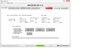
    Coming to the DAC configuration, we have configured the DAC as per the guidelines(Steps 1-2-3) in the DAC EVM Userguide, we are checking output at the J2 connector and the DAC isn't generating any output signal/tones. Image having a reference configuration attached below

    Configuration_overview

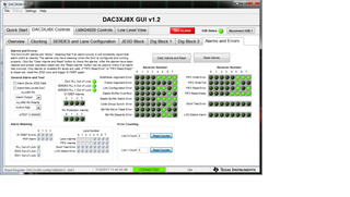
    Monitored the alarm and Errors flags in the GUI, these look to be fine(reference image attached below)Error alarms window

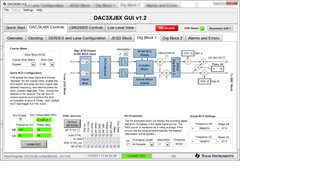
    We enabled Mixer & NCO in the GUI with frequency options on Channel AB and CD, even with this the output on J2 still remains nil. Even if we say JESD has issues in transferring the data, the NCO signal should have appeared on the DAC output (Tried with "Zero data when JESD Link not established" option ticked and unticked also), but we don't see a valid output here as well. Reference image of GUI configuration is attached below (please ignore DAC output rate SPS used while taking this screenshot)

    mixer_block_not_working 

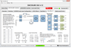
    Only the option which is giving some signal @ the DAC output is "Enable A" is ticked under "Dither" along with "Fs/2 Mixer" ticked in "Dig Block 2", this resulting in a DAC output @ FS/2 frequency. An image is attached below for reference

    only_working_option

    We probed ALARM Test point for checking PRBS errors (by proper configurations in the FPGA (31 bit PRBS) and GUI) ALARM signal was Low for all the combinations of 7-bit, 23 bit and 31 bit patterns selected in GUI, so not seeing a consistent behaviour of the Alarm pin as well. Is this pattern checker status available as a status in GUI? or are there any register status bits for this purpose?

    Could you please tell us what could be the issue here and what could be the methods to move ahead? Please provide your valuable inputs on the same.

    Thanks,
    Kiran

  • Kiran,

    When I tested this setup using Xilinx IP, I was required to send both a core clock and reference clock to the FPGA. Does your firmware require this and are you providing both of these clocks if needed? 

    Is the PLL2 Locked LED D7 on? This is required. This indicates the LMK is programmed properly when using on-board clock mode.

    Is JP1 shunt on pins 1-2? This is the TXENABLE and this must be tied high to get an output.

    Can you run the test in the attached file and verify you get a 100MHz tone out?

    Is SYNC going high and staying high after the DAC is initialized and reset?

    Regards,

    Jim

    6354.DAC38J84 100MHz NCO Test.pptx  

  • Hi Jim,

    Thanks for the quick response, Please find my response below:

    When I tested this setup using Xilinx IP, I was required to send both a core clock and reference clock to the FPGA. Does your firmware require this and are you providing both of these clocks if needed? : We are using the GT clock from the FMC and we are able to get the Clock at the Expected frequency (Line_rate/40), this we also confirmed using a reference Clock counter in FPGA.

    Is the PLL2 Locked LED D7 on? This is required. This indicates the LMK is programmed properly when using on-board clock mode. : PLL 2 LOCKED LED is On is glowing.

    Is JP1 shunt on pins 1-2? This is the TXENABLE and this must be tied high to get an output. : Jumper position is in TXENABLE state and we have Confirmed this Jumper along with others ( like Supply to the Crystal connected to LMK etc).

    Can you run the test in the attached file and verify you get a 100MHz tone out? : Sure will go through the Document and check.

    Is SYNC going high and staying high after the DAC is initialized and reset? : Yes SYNC is going high and staying High once the DAC is initialized and Reset.

    Are there any Channel based Powerdown/Sleep registers which we might be missing to configugure?

    Thanks,

    Kiran

  • Kiran,

    Please follow the steps in the attached document and see if this helps. This generates an output when using our TSW14J56EVM.DAC39J82_421.pptx

    Regards,

    Jim

  • Hi Jim,

    Thanks for the responses.

    We tried with the settings suggested by you for generating Mixer O/P and NCO configuration, now the NCO and Mixer settings working fine, we are able to see the NCO configured frequency outputs on J2. Do these settings mean that in order to use NCO and Mixer functionality we need to feed the DAC with Offset Binary Data? Won't this work with 2's Complement data?

    However, with the actual data from FPGA, we are still unable to get DAC o/p, even after the "3 step initialization sequence" from GUI, following are our observation

    • The Alarm window is showing "FIFO Read Empty" on 4 lanes (On receiver no 0,1,2,3)
    • config2 : "zero_ invalid_data" is set to "1"
    • config74 :
      1. SerDes lane0 enable, SerDes lane1 enable, SerDes lane2 enable, SerDes lane3 enable: all are "0" (Even though these options are "Ticked" in the GUI
      2. init_ state: "1111"
      3. jesd_ reset_n : "0" (this should be "1")
    • config76: is set to 0x0000, it should have shown 0x1303 (as these were our configurations)
    • Manually wrote above settings with valid values, still unable to get DAC output

    Regarding Clock Generation, it is getting generated properly and we are able to observe it be fine.

    Is there a way to confirm that the JESD Rx is UP in DAC and is in running(Some kind of Link UP or Initialization Done) status? Also, the Config registers not reflecting the GUI configured parameters could be the issue? Please provide your feedback.

    Thanks,
    Kiran

  • Kiran,

    The NCO will work with either format. This test just used offset binary since the constant DAC input is 0x0000 by default.

    Config2 is fine with a setting of 0x2002.

    Config74 must be set to 0x0F21 after initialization has completed. During initialization, you should write the following to this address:

    0x0F20, 0x0F3E, 0x0F3F and 0x0F21.

    Config76 must be set to 0x1303. Not sure why you mentioned 0x0000.

    The FIFO read empty usually means the clock frequency is incorrect inside the FPGA. Can you run Chipscope and verify the FPGA is sending the ILAS data followed by valid data on all four lanes after SYNC goes high? 

    Is SYSREF continuous or pulsed in your setup? If continuous, at what frequency?  

  • Hi Jim,

    Thank you for the response again.

    Sysref is pulsed and is not continuous in our setup.

    Regarding the register values mentioned in the previous thread, these are the register values read  after the GUI RUN initial configurations. May be few of these registers are getting configured incorrectly by the GUI Disappointed

    We will check whether ILAs are sent until Sync asserts. As I recently received access to TI reference design with the IP, we will attempt with this as well.

    Thanks,

    Kiran

  • Kiran,

    I am using the same GUI and these are the settings I am getting. Not sure why they would be different with your setup. 

    Make sure you are sending at least 3 pulses of the SYSREF. 

    Jim

  • Hi Jim,

    We confirmed using Chipscope that the JESD core is sending ILA (0xBCBCBCBC) until the assertion of Sync signal and once Sync is asserted, we also see proper data stream going to the Treanciver tile.

    IN LMK settings, with DCLK source set to "Divider", SerDes PLL0 out of lock Alarm is OFF now, but still seeing FIFO read Empty flag.

    We reconfirmed JESD settings, clock etc In the FPGA side as well, our issue is almost similar to the issue mentioned in e2e.ti.com/.../dac38j84evm-once-reset-dac-fifo-read-empty-but-still-assert-sync-after-sysref

    But we are unaware of the solution for the above-mentioned thread (Already confirmed settings like JESD lane rate, clock etc)? Are you aware any such scenarios?

    Thanks,

    Kiran 

  • Hi Jim

    Another point I forgot to mention is, SERDES PLL 1 is still "Out Of Lock", Is this Alarm Valid for the DAC in 4 Lane mode?

    Thanks,

    Kiran

  • Kiran,

    No. Only SERDES PLL 0 is used. Make sure this one is locked. 

    What value are using for K in the FPGA?

    Can you send your DAC register settings and I will try them on my setup? 

    Which output are you monitoring from the DAC evm? Only two of them will have an output.

    You can order a TSW14J10EVM and run this setup using our tested firmware.

    Regards,

    Jim

  • Have you tried the TI JESD204B/C IP yet?

  • Hi Jim,

    With TI JESD core also it didn't work, Sync is continuously toggling with this setup (LMFS = 4 2 1 1). We are using Reference clock(FMC pins D4, D5) = Line rate/40 and the Core clock is not present.

    With slac690c migrated to KC705, we are not seeing any errors but lane initialization is failing and Synch is becoming '0' after the ILA phase. Here very weird observation was incorrect Lane ID filed during ILA_CONFIG phase (Reference got from this link).

    With 2 JESD lines (LMFS = 2 2 2 1 ) we are able to generate output and bring up the setup. This is the only working setup with KC705+DAC EVM.

    For KC705 setup, with the below configurations, can you please provide us the LMK and DAC configuration files which we could directly load to DAC3XJ8X GUI (v1.2). 

    DAC Data input rate = 614.4 MSPS, Interpolation = 1, No of SERDES lanes = 4, SERDES line rate = 6144 Mbps. We are using Reference clock(FMC pins D4, D5) = Line rate/20 and Core clock (FMC pins G6,G7 ) = Line rate/40.

    Thanks,

    Kiran

  • Kiran,

    Are you still having issues with this interface?  

    Regards,

    Jim

  • Hi Jim,

    We couldn't solve the issue with KC705, it was always stuck in ILA with 4 JESD lanes setup.

    We migrated to ZCU106 setup with the Sync signal using a Jumper/Wire, there were some initial hiccups, and later on with the clock and reset recommendations as per this comment in the Xilinx forum, we were able to bring it up in 8 lane mode and it's working fine.

    We are having few other issues as mentioned in this link which we are looking into now.

    Thanks,

    Kiran