This thread has been locked.
If you have a related question, please click the "Ask a related question" button in the top right corner. The newly created question will be automatically linked to this question.
This is a continuation of the question below.
e2e.ti.com/.../tusb7320-cannot-connect-usb-2-0-devices
In the third part, the problem that PCIE was not connected with TUSB7320 reoccurred.
I would like to confirm something.
1.
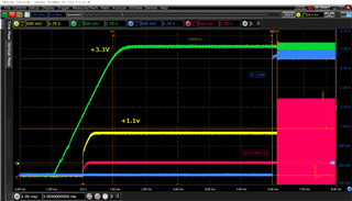
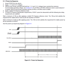
Please check the power supply startup of 3.3V and 1.1V.
Could you please comment on this waveform?
The point of concern is that 1.1V has started up first, but 3.3V has started to rise first.
2.
If PCIE communication is not possible, please tell me how to detect it on the PCIE host side.
I think there are some registers that indicate errors.
3.
Please tell me how to retry when PCIE communication is not possible.
I activated GRST and PERST but it didn't reboot.
Please let me know if there is a signal to reenter other than reset.
ok, I will look at waveform again.
Did you send unit to TI for ATE test ?
Regards
Brian
Thank you for answering.
I haven't sent it to ATE yet.
Please let me confirm two points.
1.
Please confirm the relationship between the following errata and PCIE defects.
Our circuit configuration is
WAKE#: 4.7kΩ pullup
CLKREQ#: not implemented
The rise time of WAKE# is 1 to 2 us, but here is the result below.
PCIE connected (OK)・・・1.872ms
PCIE is not connected (NG)・・・1.846ms
If there is a problem with the circuit configuration, please leave a comment.
-------
2.
Regarding the PCIE connection configuration this time, a bus switch is inserted between the TUSB7320 and the host controller.
Model number: HD3SS3212RKSR (TI)
I am attaching the circuit diagram.
Could you please comment on the control timing of the SEL terminal of the bus switch?
for Q2: only need AC cap on one side of Mux.
prefer to turn on Mux before turn on TUSB7320.
Thank you for answering.
Which part is required only on one side?
Please make a comment, such as showing it in the attached circuit diagram.
Regards
Yoda
the relationship to PCIe errata is low since only 2/1000 failed. but coatomer can try by placing a 0.001-µF capacitor on the WAKE# and/or CLKREQ# signal to ground,
Best
Brian
Thank you for answering.
I will try the WAKE capacitor.
Regarding the matter on one side, is it correct to understand that the capacitor in the figure (blue) is not necessary and is directly connected?
Regards
Yoda
You answered that you turn on the Mux before turning on the TUSB7320.
What do you mean by "turn on", such as turning on the power and canceling the reset?
Also, does this requirement apply to the host controller to which the TUSB7320 is connected?
Please tell me about the timing of the reset.
In the 9.1.1 Power-Up Sequence of the datasheet (SLLSE76N – MARCH 2011 – REVISED AUGUST 2022)
Please let me know if there is a maximum specification for the red line (minimum of 100us, minimum of 100ms).
-------
Could you please answer the following question that I asked before?
3. Please tell me how to retry when PCIE communication is not possible.
I activated GRST and PERST but it didn't reboot.
Please let me know if there is a signal to reenter other than reset.
--------
Implemented a capacitor in WAKE#.
No improvement was seen.
Regards
Yoda
For multiple questions, could you please answer the ones that you can answer?
Regards
Yoda
I have an additional question.
Please let me know if there is any problem with this waveform at startup.
In particular, I am concerned about the DC level signal generated before the GRST reset is released, which is enclosed in the white frame.
I have attached the waveforms(Attached waveform.pdf) of the boot successful and the boot failed that occurred with the same part (TUSB7320).
Could you give us a comment from the waveform?
Regards
Yoda
1: can you remove c3602/C3603 and test again?, no cap needed on RX .
2: Please let me know if there is a maximum specification for the red line (minimum of 100us, minimum of 100ms).
no max spec.
Best
Brian
Thank you for answering.
Regarding the matter of removing C3602/C3603, after removing, do you try connecting the jumper directly?
If that is the case, check if RX allows the absence of a capacitor as a specification on the host side, and then implement it.
Regards
Yoda
My question is, when do you expect to receive an answer?
If possible, I would like a reply by the morning of June 8th.
Thank you for answering.
What do you expect by replacing C3602/C3603 with 0 ohms?
Could you please answer the other two questions below?
1.
Please let me know if there is any problem with this waveform at startup.
In particular, I am concerned about the DC level signal generated before the GRST reset is released, which is enclosed in the white frame.
I have attached the waveforms(Attached waveform.pdf) of the boot successful and the boot failed that occurred with the same part (TUSB7320).
Could you give us a comment from the waveform?
2.
Please tell me how to retry when PCIE communication is not possible.
I activated GRST and PERST but it didn't reboot.
Please let me know if there is a signal to reenter other than reset.
with C3602/C3603 , the tota AC cap value on RX channel is over the spec
1: I can't see difference from waveform between two.
2: need to check with system.
best
Brian
Thank you for answering.
Does exceeding the specification of the AC cap mean that 0.1uF has a large capacitance?
Please let me know if there is a recommended value.
1.
I'm not asking about comparing waveforms.
In particular, I am concerned about the DC level signal generated before the GRST reset is released, which is enclosed in the white frame.
2.
What information should I provide to verify the system?
Regards
Yoda
ac cap should be 75 nf to 265 nf. if there are two 100nf cap in the channel, total will be 50nf..
regarding DC voltage, it's around 1.2v, which is within RX spec,0.-1.2v
Best
Brian
Thank you for answering.
The capacity of the capacitor is 0.1uF (100nf) for each of the P side and N side.
What do you mean by two?
Regarding the DC voltage, regardless of the state of GRST, does it matter if it does not exceed the range of 0V to 1.2V?
Regards
Yoda
Yoda:
I mean you have 100nf on RX side and another 100nf from TX side of CPU of SOC.
for DC voltage, 0-1.2v should be ok.
Best
Brian
Thank you for answering.
I am attaching the schematic again.
I will explain where the capacitor is connected.
Host controller → TUSB7320: C3621 (P side), C3622 (N side): Blue frame in circuit diagram
TUSB7320 → Host controller: C3602 (P side), C3603 (N side): Red frame in circuit diagram
Capacitors are not mounted for parts not shown in the circuit diagram.
Could you tell me if there is a reason why I can not answer the following question that I asked before?
2.
Please tell me how to retry when PCIE communication is not possible.
I activated GRST and PERST but it didn't reboot.
Please let me know if there is a signal to reenter other than reset.
Regards
Yoda
There was a new phenomenon related to this bug.
Could you please comment on the attached waveform?
I checked the waveforms of VDD11 and VDD33 at power-on.
When it fails, VDD11 and VDD33 seem to oscillate. (White frame of waveform at failure)
1. Please tell me about the factors of this symptom.
2. I would like to ask you again. Is there a power up order for VDD11 and VDD33?
3. Are there any restrictions on the slew rate at startup for each power supply (VDD11 and VDD33)?
4. The inrush current (red frame in the figure) is between 1.5A and 2.2A for both success and failure.
Please tell me the current value (maximum) of VDD11 that supplies the TUSB7320.
5. Is there no problem even if an inrush current (framed in red in the figure) occurs?
I would like to receive an answer today (June 15th).
Regards
Yoda
Yoda:
the noise on supply definitely could cause device power on failure, looks like something oscillating inside the chip.
There is no power on sequence for 1.1v and 3.3v, other wise it will cause lot more power on failure, not 1 or 2 of 1000 times.
ramp time should be 0.2ms to 100ms should be ok.
max current of 1.1v is 600ma, 115ma for 3.3v for 2 SS device running,
are there ferrite bead on 3.3v and 1.1v supply?
Best
Brian
Thank you for answering.
About 1 out of 1000 failures, 2 out of 1000 failures is not a small number.
In the board that occurs, it fails about 6 times in 10 times.
VDD11 and VDD33 are not attached for ferrite beads.
VDDA_3P3 is attached. BLM18EG221SN1D (Murata)
The answer was that it seemed to oscillate inside the chip.
Could you tell me if there are any factors that cause oscillation other than the order of powering on 1.1V and 3.3V and the ramp time of the power supply?
【Additional question】
Could you tell me the voltage regulation for the lamp time?
Could you tell me what "2 SS device running" means?
Regards
Yoda
This oscillation seems to have a problem with turning on the power.
Could you take a look including the power supply circuit that is supplying it?
Attached is the schematic of the power supply and the power-up waveform.
Power component: TPS74401RGWR (TI)
Input: 3.3V, Output: 1.1V
Supplement: 1.1V [VDD11] is generated from the power supply used for VDD33.
1. Please comment on the timing and slew rate from the rising waveform of the TPS74401.
2. Does the 600mA maximum current for VDD11 include inrush current?
3. Are ferrite beads required for VDD11 and VDD33?
What characteristics, if any, would be best?
4. Is slow start required when using the TPS74401RGWR?
5. What is the voltage ratio specification (0-100% or 10%-90% or 20%-80% etc.) for the slew rate of the power supply?
I would like to receive an answer today (June 16th).
Regards
Yoda
Yoda:
Can you send schematic for power supply part for .3v and 1.1v?
Best
Brian
The number of error occurrences changed by changing the parts of the power supply circuit.
I attach each correction method and waveform.
Could you please comment?
I would like to receive an answer today (June 19th).
Regards
Yoda
Could you please answer the question?
Schematics for 3.3V and 1.1V power supplies are available upon request.
I would like to receive an answer today (June 20th).
If it is difficult, please let me know the date when you can reply.
Regards
Yoda
Yoda:
It seems if 1.1v supply is ramp after 3.3v is stable., no error found. This is very good data .
best
Brian
Thank you for answering.
Is it recommended that the TUSB7320 power-up sequence is to ramp the 1.1V supply after 3.3V has stabilized?
Regards
Yoda
Thank you for answering.
Where in the datasheet are you trying to update the power sequence?
Regards
Yoda
Thank you for answering.
I know it fixes section 9.1.1.
Could you tell me which part to fix specifically?
For example, I think that there is a need to add order regulations and time regulations to the startup of the power supply.
I have not received any answers to my questions so far. I would like an answer.
1.
Oscillation occurs in the chip when an error occurs.
Could you please explain what happens inside the chip when it oscillates? I don't know what causes the oscillation.
2.
What is the voltage percentage specification (0-100% or 10%-90% or 20%-80% etc.) for a slew rate of 1.1V (VDD11)?
Changing the slew rate changes the frequency of error occurrence.
I want to check the regulations.
3.
Does the 600mA maximum current for VDD11 include inrush current?
I am concerned about damage to the TUSB7320.
4.
Please tell me how to recover when an error occurs.
For example, reset on, power on again, etc.
5.
Improvements can be seen by changing the slew rate of the power supply.
What is your recommended circuit plan for designing the TUSB7320?
I would like to receive an answer today (June 21th).
Regards
Yoda
1: There is PLL inside chip, we suspect the PLL circuit may not work properly if 3.3/1.1v supply power on sequence not meet requirement.
2: slew rate is 10% -90%.
3: 600mA maximum current for VDD11 does not include inrush current.
4: if error happens, you need to re-do power on reset.
5: For slew rate, suggest to power on 1.1v supply after 3.3v stable.
Best
brian
Thank you for answering.
I would like the order rules for power-up to be described in the datasheet or errata.
In the current data sheet, it is not possible to read the order of power supply start-up of 1.1V and 3.3V and turning on the 1.1V power supply after 3.3V is stabilized.
I would like to receive a timing chart when designing the power supply input to the TUSB7320.
Regards
Yoda
current data sheet based on no power sequence.
sure, we will include timing chart in the new dtasheet.
best
Brian
Thank you for answering.
Please let me know what part of the datasheet to correct (for example, power up time).
The current datasheet doesn't tell me how to design to avoid the bug.
Please let me know when the datasheet will be revised.
Regards
Yoda
Yoda:
We are going to update section 9.1 power up sequence.
I expect the datasheet will be revised by two weeks if we start this week. But I need to check to make sure.
Best
Brian
It's confirmed.
Can you solve the problem that PCIE does not output by correcting the datasheet?
Regards
Yoda
Thank you for answering.
Please release the revised datasheet as soon as possible.
Regards
Yoda
Another event occurred due to a problem at startup.
Could you please comment on this incident?
Regarding the operation of the TUSB7320 at startup, a waveform with a cycle different from the standard is output from the USB CHIRP signal.
The frequency of occurrence is very low, about 1 in 2000.
It is different from the part that occurred due to PCIE failure.
Please refer to the attached file for measurement points and waveforms.
Regards
Yoda
Yoda:
What is power on sequence for this test condition? PLL was locking to a wrong frequency.
Regards
Brian
Thank you for answering.
The waveforms of VDD11, VDD33, GRST, and 48MHz are attached as the startup sequence of the defective board.
I would like to know what could be causing the PLL to lock on the wrong frequency.
As for GRST, it seems to go around from the inside when the TUSB7320 powers up.
In the attached waveform, it has started normally.
Regards
Yoda
I sent you the waveforms, but could you please comment on the startup sequence?
Also, regarding the frequency of occurrence, at low temperatures (Celsius:5°C), the number of occurrences increases to about 15 times out of 400.
It's been two weeks since I received your notification regarding the revision of the datasheet due to the PCIE defect.
Could you tell us about your progress?
Regards
Yoda
Yoda:
Can you try to turn on 1.1v after 3.3v stable?
for datasheet, it may got delayed due to holiday last week, but still in process.
Best
Brian