Part Number: TUSB211A
Tool/software:
Some USB2 redrivers do not need to be directly integrated into a trace, and can just be placed over the trace. Why is that? Won't this cause the signal to not be boosted?
Part Number: DS280DF810EVM
Tool/software:
In this FAQ, I will explain how to reflash a USB2ANY device to interface between an EVM board and SigCon Architect GUI. This FAQ applies to any EVM which is controlled by a USB2ANY with SigCon Architect GUI. This is a good debug step to take if you are having trouble connecting to your EVM through the GUI.
Part Number: DS125DF111
Tool/software:
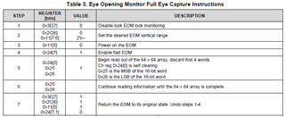
In this FAQ, I will cover the SMBus register sequence to capture a full eye opening measurement. This FAQ applies to the following part numbers:
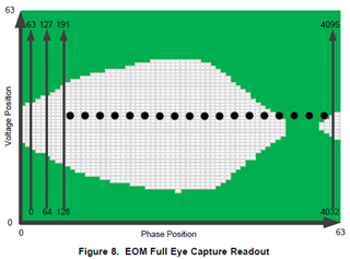
To capture the full eye opening measurement, follow the instructions in the table below.
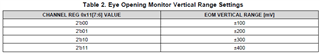
In step 2, the EOM vertical range can be configured with the following values.
Step 5 can be explained in greater detail with the following sequence.
Part Number: DS320PR810
Tool/software:
Hi All,
Texas Instruments uses PCIe redrivers to perform signal conditioning on medium to upper medium loss systems. The redriver is effective in a wide variety of systems with losses ranging from -36dB to -56dB. As a result, the tuning that needs to be done to maximize the margin between the endpoint and the root complex is very fine and often can have multiple possible options. Additionally, there is another layer of complexity in the form of DC gain because certain links will need a small amount of amplification or reduction for improved margin. The difficulty becomes then, how does one find the optimal setting for the redriver tuning position?
Although there are many tools (IOMT, AMDXIO, PCI_LMT) that can provide margining information at the CPU and sometimes at the endpoint in the form of eye height in mV and eye width in UI, there is only one tool that can provide information at the output of our redriver, and that tool is eyescan.
Eyescan provides a histogram from a DAC sweep measurement at the TX of our redrivers. Imagine there is a horizontal line moving vertically upward on an eye diagram. At the lower end of voltage, in the -300 to -400 mV range, there will be 0 hits. This is because no bit transitions are reaching this level of voltage. Then, the DAC moves up a step. The steps can be 12.5mV, 9.375mV, 6.25mV, and 3.125mV. After it moves up the amount of the step, it then counts the hits at that level. This time, there are 400 hits. The horizontal line has reached a point where the bit transitions are accumulating. But, why are the bit transitions accumulating at this point? Well, you can divide an eye diagram into 3 main parts. 1 is the low level position 2 is the high level position and 3 is the transition between those positions. In an eye diagram, the low level and high level positions will be points of accumulation for data. This is because as data is transmitted, the majority of the time, it is either 0 or 1. Back to the eyescan and the DAC step. The reason that there are now 400 hits is that the horizontal line has now hit the low level position. It will then continue moving up the eye and measure the hits at each mV height of the low level position. Eventually, it will move into another portion of the eye diagram, the transition between the levels. At this point, it can then sample the eye itself. In the eyescan, this looks like a flat portion. Below, is an image of an eye scan where the flat portion is visible.
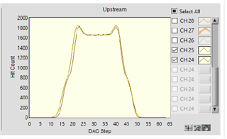
Notice how there is a flat portion in the waveform. The horizontal line is moving between the high and low positions. The amount of steps between those two peaks can be thought of as the eye height. Somewhere in the middle of the number of DAC steps required to sample the entire eye, there is the center of the eye. The horizontal line continues upwards, in step intervals denoted above, and reaches the high level position. At first, it registers a higher amount of hits. This can be seen as the small upward bumps at the corners of the waveform. There are more transitions here because there is an accumulation of hits around the high level position. The DAC continues upwards and moves through the high level position just as it does with the lower level position.
Please ensure you understand the functionality of the eyescan before continuing and then see these conclusions:
Best Regards,
Nick
Part Number: TDP2004
Tool/software:
What is Dual Mode
Dual mode or DP++ allows for a DP source to output a HDMI signal to a sink without using an active protocol converter. The DP source must be DP++ capable for dual mode operation. The key considerations when designing a dual-mode system is the AUX/ DDC bus connections on the source, and the main link connections for the DP signal.
Main Link Connections
The main links of the DP++ source will be mapped to the DP++ connector as follows.
|
DP Source Output Pins |
DisplayPort Receptacle Pins |
|
ML_Lane_0 (n) |
ML_Lane_0 (n) |
|
ML_Lane_0 (p) |
ML_Lane_0 (p) |
|
ML_Lane_1 (n) |
ML_Lane_1 (n) |
|
ML_Lane_1 (p) |
ML_Lane_1 (p) |
|
ML_Lane_2 (n) |
ML_Lane_2 (n) |
|
ML_Lane_2 (p) |
ML_Lane_2 (p) |
|
ML_Lane_3 (n) |
ML_Lane_3 (n) |
|
ML_Lane_3 (p) |
ML_Lane_3 (p) |
|
AUX_CH (p) |
AUX_CH (p) |
|
AUX_CH (n) |
AUX_CH (n) |
|
DP_PWR |
DP_PWR |
|
Hot Plug Detect |
Hot Plug Detect |
|
CONFIG 1 |
Cable Adaptor Detect |
|
CONFIG 2 |
HDMI CEC |
AUX/ DDC Connections
AUX and DDC are the video status and control busses for DisplayPort and HDMI respectively. The AUX interface is an AC coupled interface that communicated over 1Mbps Manchester encoded data. The DDC interface is a DC coupled interface that communicates via I2C, so pullups may be required.
As you may have noticed the DDC and AUX protocols are incompatible and must be gated so only one is active at a time. In the dual mode spec there is a cable adaptor detect (CAD) pin which can determine if a DP or HDMI sink is connected to the dual mode source. This CAD pin can be used as the control for the gating between the DDC and AUX bus.
An example implementation on DP++ AUX/ DDC can be seen below-.
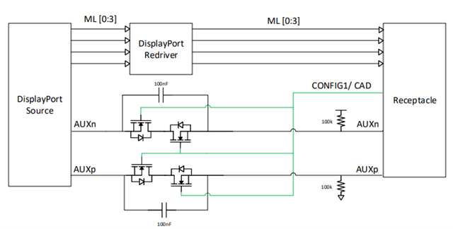
This implementation takes advantage of the switching properties of a MOSFET keeping the MOSFET open when CAD Is 0, and bypassing the capacitors when CAD is 1. This will allow for the AC coupled AUX signal to pass when a DP sink (CAD = 0) is connected to the system, and the DC coupled I2C signal to pass when a HDMI sink (CAD = 1) is connected. A key assumption in this implementation is that the required 3.3V pullups for I2C communication are placed on the HDMI sink DDC lines.
Part Number: DS320PR810
Tool/software:
TI PCIe Gen 5/Gen 4 redrivers have powerdown (PD or PWDN) pins. How should I configure them, and why does TI suggest connecting them to inverted PERST# or PRSNT#?
Part Number: SN65DPHY440SS
Tool/software:
I'm utilizing the SN75DPHY440SS in 4 lane configuration with default configuration parameters, sourced by a CSI-2 source. Lanes 1, 2, and 3 are correctly driven and re-drive both LP and HS signals.
Lane 0 is driven by the same source but fails to pass HS data (oddly, LP data is being passed correctly).
This "shouldn't" matter, but we are NOT abiding by lane ordering (i.e. MIPI lane 4 passes through DA0P/DA0N) - per the datasheet, that's acceptable.
Source receiver and termination is identical for each lane.
Any thoughts or similar experiences?
Part Number: TUSB1142
Tool/software:
The TUSB1142 design uses the Flip signal from a TPS25820 to switch the SuperSpeed signals from a USB Type C connector. We are not able to get SuperSpeed to work at all.
Part Number: DS280DF810
Tool/software:
Introduction:
One common debug question when using TI's 25G/28G is why is the PRBS generator not working? This FAQ will review the key criteria for the retimer PRBS generator to function.
Retimer Architecture:
TI's 25G/28G retimers implement a "referenceless" CDR architecture. This means that the clock used for retiming data in the retimer is solely based on the recovered clock from the data the retimer receives. The 25 MHz calibration clock required for these retimers is just used to set the VCO to the correct approximate frequency for CDR lock, but is not used as a reference clock for retiming the data.
The recovered clock signal from the retimer is required for the PRBS generator to function. This can be seen in the block diagram of DS250DF410, shown below.

Using Retimer PRBS Generator:
A key requirement of using the retimer PRBS generator on a given retimer channel is for that channel to have CDR lock. There are two primary means of accomplishing this:
1) Provide a data input to the retimer, such as 25 GbE data.
2) Provide a sub-rate clock input to the retimer.
A sub-rate clock input is a low frequency clock signal intended to look like a series of repeated 0s and 1s to the retimer. As an example, in order to create a 25.78125 Gbps PRBS output from the retimer, a 1.611328125 GHz clock signal can be supplied to the receiver. This frequency is derived from 25.78125 Gbps / 16, which looks similar to a data pattern of 0000000011111111. For the clock amplitude, use an amplitude that matches supported receiver input amplitude range. TI often uses 800 mVppd clock input.
Beyond ensuring that a valid signal is present on the retimer receiver, it is important that the retimer CDR data rate and PRBS generator are configured correctly. Details on configuring these parameters can be found in the 25G/28G retimer programming guide, found in the corresponding retimer secure folder. Additionally, the SigCon Architect GUI combined with the appropriate device profile can be used to accelerate device configuration.
Part Number: TUSB211A
Tool/software:
In order to perform eye-diagram testing, the TUSB211A and other USB 2.0 redrivers must first detect the scope termination after power on or reset. Once termination has been detected, then the redriver will enable the boosting feature to take the eye-diagrams correctly.
More details are provided in Section 8.2.2.1 of the TUSB216 datasheet.
