FAQ: Logic and Voltage Translation > Quality and Manufacturing >> Current FAQ
TI's General Quality Guideline (page 7) describes our official policy on obsoleting a device. This policy is summarized below.
FAQ: Logic and Voltage Translation > Voltage Translators >> Current FAQ
Some of the TI translators have requirements during normal operation mode to have Vcca <= Vccb ( TXS/ TXB01xx) or Vrefb>= VrefA+0.8V(LSF). However, the TI translation devices do not specifically have any power sequencing requirements (power up and power down).
Usually, the datasheet’s power supply section mentions if there are any power sequencing recommendations. Note that the power sequencing can be modified according to the needs of the application/system without any performance or reliability concerns to the device.
In general, TI recommends having the ground connected before any supply is applied while the control and I/O ports are preferably at ground through weak pulldown resistors
Refer to the AXC app note which doesn’t require any power sequencing:
FAQ: Logic and Voltage Translation > Logic Technology >> Current FAQ
The IOFF specification guarantees the I/O ports are in high impedance whenever either one of the power supply is at pulled to ground (0V) or close to gnd(<100mV as specified for the AXC devices). The Ioff is not guaranteed when the power supply is left floating. The Ioff spec is listed in the datasheet electrical specs table.
Detailed information about live insertion with our logic devices can be found in the Logic in Live-Insertion Applications application report
Vcc isolation is a feature of the devices which support the Ioff partial power down spec.
An important point to note is that the input buffers of the I/O ports of the powered up supply side are still active and this can lead to high power consumption with floating inputs. For e.g. For any device which supports Ioff, if Vcca is 0V, and Vccb is at 5V, then the B ports must not have floating inputs. Similarly, if Vccb is 0V, and Vcca is at 5V, then the A ports must not have floating inputs.
TI recommends having weak pulldown resistors to limit higher than normal Icc current, whenever the Vcc isolation feature is considered to be used in the application.
FAQ: Logic and Voltage Translation > Voltage Translators >> Current FAQ
For the TXB family, unused I/O ports are recommended to be tied to GND through a weak pulldown resistors (>=100kohm).
For TXS devices, the internal 10kohm pull-ups resistors will ensure that the I/O ports are never floating and hence can be left disconnected.
For LSF devices, the unused I/O ports can be left disconnected as they are passive switch type translators.
For AVC/LVC/TXV devices, the unused input and output ports are recommended to be tied to gnd.
For AXC/LXC devices, the unused input and output ports can be left unconnected as there are very weak pulldown resistors internally. This helps in avoiding unknown voltages at the pins thus reducing the power consumption due to floating voltage levels.
FAQ: Logic and Voltage Translation > Monostable Multivibrators >> Current FAQ
To make a long post short: MMVs cannot be directly simulated by PSpice because of their direct dependence on external components. We recommend prototyping instead of simulating.
The remainder of this post is explaining why.
Monostable Multivibrators (MMV -- aka "one-shots") are particularly challenging to reproduce in PSpice due to their internal complexity and their dependence on external components.
It is possible to simulate the device by representing every semiconductor component inside the device, however the simulations created this way are slow and the PSpice circuit would give direct access to TI's intellectual property.
The method used to simulate most devices in PSpice is to represent their behavior rather than their internal structure. This is known as a "behavioral PSpice model" and is the more common form of model that we make publicly available.
MMVs use external timing components, namely one resistor and one capacitor, to produce a pulse of known width at the output. We can simulate this process with decent accuracy, however there is a large problem.
Every MMV has what's known as a "K" factor. This value directly influences the output pulse width, per the equation:
tw = K*R*C
Here's an example plot of the K factor taken from the SN74LVC1G123 datasheet:
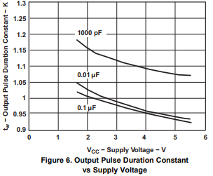
As you can see, the K factor is dependent on two values -- supply voltage, and timing capacitor value.
This dependence on the external component's value is what makes PSpice modelling so difficult. PSpice doesn't provide a method to grab the external capacitor's value from a circuit to produce the appropriate K value.
Unfortunately, as long as this is the case, an accurate MMV behavioral PSpice model will not be available.
(1) Start with the required pulse width tolerance. If your end system can't handle ~10% change in the pulse width, I would recommend against using an MMV for the solution. Other more accurate solutions are probably better for your situation.
(2) Use the given K values in the datasheet values to calculate the necessary RC value via this equation:
RC = tw/K
(3) Start by selecting the C value as 0.1uF (one of the most common capacitor values avilable, typically used on every board for decoupling capacitance), then calculate R from that via the equation:
R = RC/C
(4) If R is found to be larger than 1 MΩ or smaller than 1 kΩ (or 5kΩ at 2V operation), repeat step (3) with a larger or smaller capacitor until a resistance in the appropriate range is found.
(5) Build a prototype with the found values and the exact components planned for use in the final design. Test the pulse width output across your expected operating temperature.
(6) It's likely that there will be some variation from the calculated values to the prototype. Adjust the resistor value to compensate.
It's important to note that an MMV isn't a very precise timing instrument. It is really intended as a low cost solution to provide a pulse that's "close enough" to the required width. If really accurate pulse widths are required, there are other options out there that will get you better results (for example, crystal oscillators and MCUs)
FAQ: Logic and Voltage Translation > Logic Technology >> Current FAQ
Hi Team,
May I know difference is there between mux/demux IC's and analog switch IC's?
I'm comparing this in the context of chips with the same IO lines (for example a 1:2 or 2:1 mux/demux vs. a SPDT analog switch).
Regards
Hari
FAQ: Logic and Voltage Translation > Output Parameters >> Current FAQ
The high logic level output voltage of a logic device with no load will be the supply voltage.
The output current of a logic device is determined by the load connected to the device and the strength of the output driver
It's important to note that VOH or VOL is always given together with a test current (IOH or IOL, respectively).
For example:
An ideal 5-V logic gate (ideal := 0 Ω output impedance) connected to a 100 Ω load will be outputting IOH = VCC/100 = 50 mA with VOH = 5 V
A more realistic 5-V logic gate with a 25 Ω output impedance will be outputting IOH = VCC/(100+25) = 40 mA with VOH = VCC*100/(100+25) = 4 V

Figure 1. Equivalent output structure for a push-pull output CMOS logic device.
The questions we get on this topic typically come in one of two forms, and I will cover each separately. Both of these are fairly complex questions that deserve more than a single FAQ post, however I will try to give a quick and easy answer to help the reader.
Assuming you keep the output current the same, the voltage _drop_ at the output will be maintained when VCC is at or slightly above the value given in the datasheet. For example, if the datasheet says the VOH at 3-V supply is 2.7V, then the voltage drop is 3 - 2.7 = 0.3V. If you change the supply to 3.3V, then it is safe to say that the minimum VOH will now be 3.3 - 0.3 = 3 V.
VOL is even easier, with the VOL remaining the same -- ie a VOL of 0.55 at 4.5-V supply will still be a VOL of 0.55 V at 5-V supply.
If you need a more precise value, linear interpolation between the given datasheet values, or linear extrapolation beyond the datasheet values, can be used to directly find the correct values. Just be sure to (a) use the closest 2 values in the datasheet to do the inter-/extra-polation and (b) hold all other values constant.
This FAQ has some additional details that may be helpful:
This is a trickier question to answer -- it appears that there is some confusion in the definition of IOH and IOL.
IOH and IOL are defined as the currents at which the VOH and VOL values in the datasheet are tested. These current ratings give a good idea of the maximum recommended output current of a logic gate, however they do not indicate a limit for the device.
For example:
A 5-V supply, 15-Ω output logic device lists an IOL of 24 mA, and a 35 Ω resistor is connected from the output to 5 V.
The current produced will not be limited to 24 mA; it will be governed by Ohm's Law: IOL = (VCC)/(15 + 35) = 100 mA.
For most logic devices, this would cause damage to the device, and likely the system.
This FAQ has some additional details that may be helpful:
-
If you need to know the maximum current ratings of a device, please refer to the Absolute Maximum Ratings table in the datasheet. There you will typically find an absolute maximum rating of current for each output and an absolute maximum rating of current total for the device (often referred to as "current through Vcc or ground")
FAQ: Logic and Voltage Translation > Output Parameters >> Current FAQ
Transmission lines cause a lot of confusion for engineers. I hope to clear up some of that here. I will break this up into a few sections, so if you already know something you can easily skip to the information you need to know.
** Just as a disclaimer, transmission lines are an extremely complex topic, and I could never cover everything related to them here. **
For the purposes of this post, a transmission line is just a wire that has been designed to carry an electrical signal with minimal loss over relatively large distances. We typically see these in a few forms:
Stripline/microstrip: these are traces on a PCB. Any trace can become a transmission line if it gets long enough. These are the most common source of issues for system designers if transmission lines effects are not taken into account.
Coax cables: These are typically 50-Ω characteristic impedance cables designed specifically for matching RF signals to 50-Ω signal sources and 50-Ω loads. There are other impedances out there, however 50 Ω is the most common version. The transmission line consists of center conductor surrounded by an insulator, and then a tube of conductive material. The signal typically rides on the center conductor and the outer conductor is grounded.
Twisted Pair: These are exactly what they sound like - a pair of wires, usually with one signal and one ground, that are twisted together to form a double helix. They are most commonly found in network cables like Cat5e. Network cables have a typical characteristic impedance of 100 Ω.
Parallel Line: These are any two wires in parallel, one with the signal and the other grounded (typically). The most common form of these is a ribbon cable, which just has a bunch of wires in parallel running from one location to another. They are not used as commonly today due to noise and interference concerns.
Generally speaking for logic? 12 cm
This value is heavily related to the frequency content of a signal, so the faster your edges are, the smaller that number gets. Let's quickly cover what I mean by "frequency content."
Any signal can be broken down into a series of sine waves, and square waves end up being an infinite series of sine waves summed together. There's a great explanation here if you're interested: https://en.wikipedia.org/wiki/Square_wave
So, in a real signal, the maximum edge rate is the primary control on the frequency content of the signal. Let's use a 1 MHz signal as an example. Here's 3 square waves that are all 1 MHz signals:
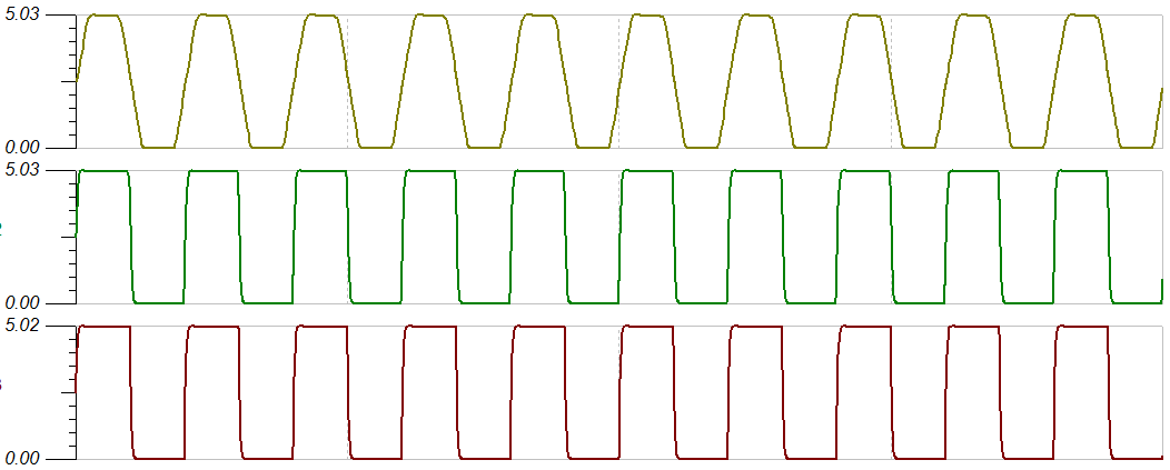
Three 1 MHz signals, each with a different edge rate. Top to bottom: 100ns, 10ns, 1ns
I took the fourier transform of these, and found that the harmonics for the first signal had already dropped below 0.5V after just 20 MHz, while the third signal still had a 0.518V component at 100 MHz.
The general rule of thumb for determining the bandwidth of a square wave is to use the transition time (t_t, 10% to 90%) of the signal in this equation:
BW = 0.35 / t_t
For the top waveform above, the bandwidth is expected to be 0.35 / 100ns = 3.5 MHz, while the last signal would be 0.35 / 1ns = 350 MHz.
This bandwidth frequency, and not the square wave frequency, is what we are referring to when we talk about the "frequency content" of a signal.
Typical logic signals have transition times between 1ns and 10ns, which puts the typical maximum bandwidth of a signal around 350 MHz.
The general rule of thumb for a transmission line to be considered 'long enough' to start acting like a transmission line is one quarter wavelength ( λ/4 ). To get wavelength we can use this equation for a quick approximation:
λ = vp / BW = 146 Mm/s / 350 MHz = 0.417 m
λ/4 ~= 10.4 cm
vp is the 'phase velocity' - aka the speed that a waveform travels in a particular transmission line. For brevity and the sake of this document, this value only depends on the relatively permittivity and the speed of light in a vacuum, and the equation is vp = c/sqrt(εr).
In the world of under 350 MHz square-wave clock signals (which is where standard logic devices 'live'), a "long distance" is at least 10.4 cm (I usually estimate at 12 cm). On many circuit boards and in many systems, 12 cm isn't that large of a distance, so you might start to see transmission line effects on your board.
Imagine an infinitely long transmission line. Connect your signal source to that transmission line and start transmitting a 5V digital waveform. How much current does the wire draw from the 5 V, 50 Ω source? The amount of current is directly determined by the characteristic impedance. For a 50 Ω t-line with a 50 Ω source and 5V signal, the current will be I = V/R = 5 / (50 + 50) = 50 mA.
Bringing that down to a realistic length transmission line (no longer infinite), the line will act like a ground-terminated resistor of the characteristic impedance value for the amount of time it takes the signal to travel down the t-line, then reflect back (at least, in the simplest case).
The characteristic impedance of a transmission line is simply the ratio of voltage to current at any point in the transmission line. The proof of this is complex, so I won't explain here, however just know that when you see "50 Ω" on a transmission line, it DOES NOT mean that the line acts like a 50 Ω resistor for DC signals. It means that the travelling waves on that line will have a ratio of voltage to current that is 50 Ω, after all, resistance as defined by Ohm's Law is just a ratio:
R = V / I
When a signal travels over a transmission line, there is typically very little loss (which is why we use transmission lines), however it takes time for the signal to propagate through the line. This time component is the primary source of issues.
From the previous section, we know that at -any point- on a transmission line, the voltage to current ratio will always be the same value (given as Z_0, aka the characteristic impedance of the transmission line).
What happens when you connect a resistor to the end of the transmission line, forcing it to have a different voltage to current ratio (say 50 Ω on the transmission line and a 100 Ω resistor at the load)?
When the ratio of voltage to current is different on the transmission line and at the load, this produces a reflected wave.
Here's 3 more square waves measured at the load, this time having different load terminations with everything else being held constant:
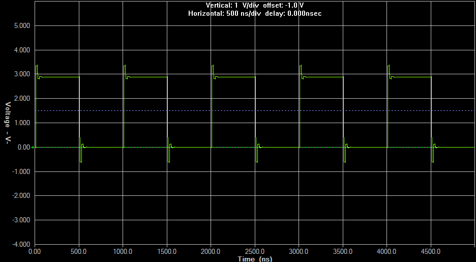
100 Ω termination, 50 Ω transmission line
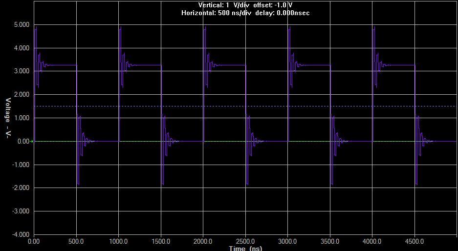
1 kΩ termination, 50 Ω transmission line
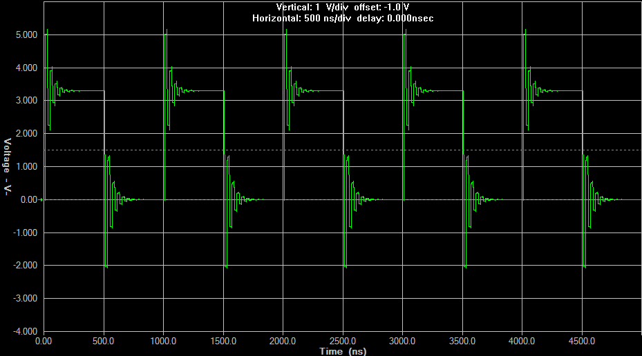
10 MΩ termination, 50 Ω transmission line (most typical impedance for a CMOS input)
You can see in the above images that the overshoot and oscillation on the line gets worse as the termination impedance gets larger. This is because the impedance match to the transmission line is getting worse. Note also that the input waveform was a 3.3-V square wave, and the output is reaching over 5 V in the last example. The reflections on the line are additive, resulting in large voltages that can be damaging to CMOS devices.
The output signal will have a delay based on the length of a transmission line. Here's an example with 3 different length lines, showing the input (red) and outputs (yellow, purple, green) in the same plot:
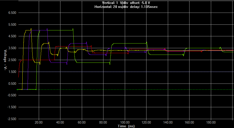
* Only the input for the green line is shown (in red), the other inputs start at the same time.
This image shows a few interesting things.
First, the input is not a clean square wave due to the reflections on the line.
Next, the delays are noticeably different for the initial rising edge of the signal.
Finally, the oscillation (aka ringing) on the signals is related to the delay. You can see that the green signal oscillated much longer than the yellow signal due to the longer delay on the line -- this is because reflections take longer to go back and forth on the line.
Some people think the best solution is to impedance match the signals. Although this will eliminate reflections, it will introduce new problems. Here's a (close to) perfectly matched impedance signal output waveform:
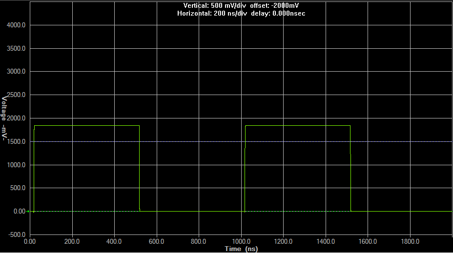
Output of 3.3V signal with matched 50 Ω input, Z_0 = 50 Ω, and 50 Ω load.
The signal looks great, however you should note that the output only reaches about half of the input voltage, which is what we would expect (50 Ω input from source, 50 Ω load... Vout = Vcc * 50/(50 + 50) = V_CC/2). This is generally a bad thing in logic circuits.
The best options that I know of is to use a damping resistor at the input to match the input as much as possible to the transmission line, as shown here:
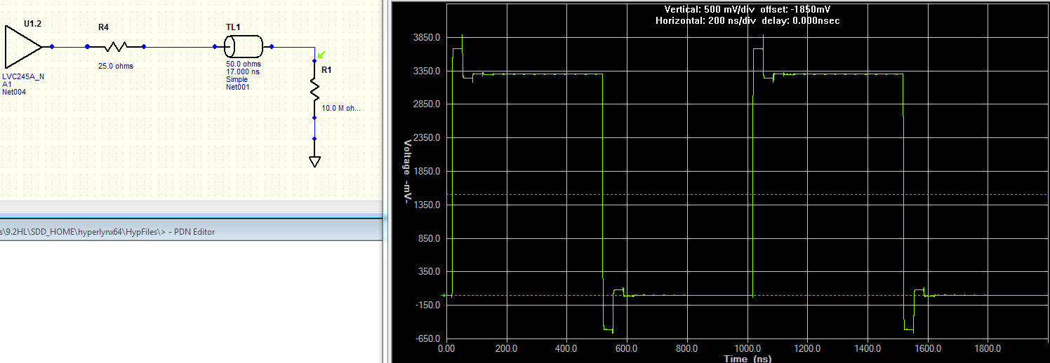
The circuit on the left shows an added damping resistor of 25 Ω. The LVC series of logic has output drive strength close to 20 Ω, so this added resistor gets us close to the required 50 Ω.
You can see in the output waveform that the ringing is significantly reduced, even though the load is still the same 10 MΩ that was used up in my first example. This signal would not cause any problems when going into a CMOS input.
This method works by eliminating the reflections on their first bounce. There is still a reflection from the high-impedance load, however the signal source is close to a perfect match, so those reflections will not bounce back and forth on the transmission line.
FAQ: Logic and Voltage Translation > Output Parameters >> Current FAQ
The primary concern with connecting outputs together is called "bus contention."
If one output is driving HIGH and the other output is driving LOW, then you have bus contention, and the device can be damaged. Here's an example with a fairly typical LVTTL driver:
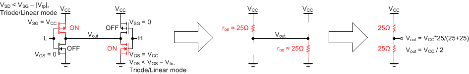
In the above image, one CMOS output is represented as a single pair of nMOS and pMOS transistors. This is a very typical arrangement for CMOS outputs.
If we use a 5V supply for Vcc, it is easy to calculate the expected current as Iout = 5/(25+25) = 100mA. The current exceeds the datasheet absolute maximum for most logic CMOS outputs, and would likely damage the device.
It is possible to parallel channels of a device to increase drive strength -- it is just important to ensure that both outputs are always in the same state. The best way to achieve this is to use two channels in the same device, and to directly connect the inputs together to ensure they will always have the same state.
FAQ: Logic and Voltage Translation > Logic Technology >> Current FAQ
The "Ioff" specification in the electrical characteristics table is only in the datasheet of devices that have the special feature of "partial power down" - also known as "back-drive protection."
Partial power down protection is the lowest level of live-insertion isolation, as defined by the application report "Logic in Live-Insertion Applications."
Partial power down essentially states that, if the supply of a device is held at 0V (any supply for multi-supply devices), then the input and output pins of said device will enter a high impedance state. The maximum leakage current in this high-impedance state is defined by the Ioff specification in the datasheet.
