

Hi TI Experts,
Is there a list of design recommendations or commonly observed errors for DDR4 / LPDDR4 MEMORY Interface during Custom board hardware design?
Thank you.

Hi TI Experts,
Is there a list of design recommendations or commonly observed errors for DDR4 / LPDDR4 MEMORY Interface during Custom board hardware design?
Thank you.
Hi Board designers,
Here are some of the commonly observed errors and recommendations for DDR4 / LPDDR4 MEMORY Interface during Custom board hardware design.
Recommendations
AM64x
DDR Board Design and Layout Guidelines
https://www.ti.com/lit/pdf/spracu1
DDR Board Design and Layout Guidelines for AM62x/AM62L can be additionally referenced
www.ti.com/.../sprad06
AM62x / AM62L
https://www.ti.com/lit/an/sprad06/sprad06.pdf
AM62Ax and AM62Px
https://www.ti.com/lit/an/sprad66a/sprad66a.pdf
Refer to the processor specific data sheet.
AM64x / AM243x (ALV)
https://www.ti.com/product/AM2432
https://www.ti.com/product/AM6442
DDR4, LPDDR4
AM62x
https://www.ti.com/lit/gpn/am625
DDR4, LPDDR4
AM62L
Note on DDR4 support for Am62L:
Refer to AM64x or the AM62x SK or EVM for DDR4 interface implementation.
DDR Configuration for AM62Lx, they can use the AM62x tool. This has the same DDR controller and PHY as AM62L
1) Currently no SDK/driver support available as there is no EVM to validate this
2) We are evaluating how to have some bare minimum support for DDR4, but this will likely be a couple of months of effort *however* even if we do this there will be no support for low power modes with DDR4 until we have a robust EVM like platform for SDK teams to offer full support
Check the documentation on TI.com for the available support.
AM62Ax
https://www.ti.com/lit/gpn/am62a7
LPDDR4
AM62D-Q1
https://www.ti.com/lit/gpn/am62D-Q1
LPDDR4
AM62Px
https://www.ti.com/lit/gpn/am62p
LPDDR4
Reference Links
(+) AM625: DDR CLK termination specification - Processors forum - Processors - TI E2E support forums
For DDR4, DQx swizzling is allowed (no register config changes are necessary). No swizzling of DM, DQS, or address is allowed.
The restriction on prime bit swapping (D0 and D8) on DDR4 is not required for any of the AM6x processor family.
4.Customer is looking for design guidance with DDR4 and not have external VTT termination Is it possible to do that?
AM62x, AM62L and AM64x with DDR4 can be designed without VTT termination as long as all signals are point to point with one load (ie, design uses one DDR4 device).
The AM62x SK is an example of this.
https://www.ti.com/tool/SK-AM62B-P1
In case you would want to add terminations follow the AM64x EVM
https://www.ti.com/tool/TMDS64EVM
it is recommended to follow the device specific EVM or SK
DDR4 clock termination
I have a question from my customer for DDR CLK termination specfication.
According to SK-AM62 schematics (PROC114E3_SCH.pdf), page#16.
DDR_CLKP/N are terminated by resisters and capacitor.
Do you have DDR termination specification?
How are these resisters and capacitor values defined?
This is actually taken from the DDR4 recommendation from Micron, in their appnote TN-40-40. Here is the quote from the appnote:
If simulations determine that AC termination is needed, terminate CK_t and CK_c through approximately 36Ω series resistors and a .01uF capacitor to VDD. A single approximately 36Ω resistor in parallel across CK_t and CK_c may also be adequate.
6.The SK-AM62B-P1 design uses a single 2GB DDR4chip. The customer now requires 4GB and 8GB . Any suggestions?
We do not support multiple loads on the DDR4 data bus, so customer would have to accomplish this with a larger density memory device. We support up to 2 x8 DDR4 devices such that each data byte has one load. For higher density you can connect 2 x8 devices in a dual rank configuration.
Verify the BG0 and BG1, CS0 and CS1 connection and ensure these are connected as per the recommendations based on the selected memory and density.
7. LPDDR4 Bit swapping for AM62A and AM62P
Refer Channel, Byte, and Bit Swapping section of AM62Ax/AM62Px LPDDR4 Board Design and Layout Guidelines
8. LPDDR4 Bit swapping for AM62X, AM62L
AM62x will follow AM62A/P for LPDDR4, DQx/DM can be swizzled within a byte, and bytes can be swapped
Refer Channel, Byte, and Bit Swapping section of AM62Ax/AM62Px LPDDR4 Board Design and Layout Guidelines
9. I plan to use TPS51200 for DDR4 and have some confusion about the REFOUT pins of the TPS51200. I found that some EVB designs use the output of REFOUT as DDR4 VREFCA, and some other EVB designs use resistor divider.
So, I wonder which way is better?
Either REFOUT or resistor divider can be used for DDR4 VREFCA. Use of Resistor Divider and filters can be avoided when REFOUT is available.
10. Do you have any recommendation for the Resistor Divider implementation
Refer below E2E:
11. SK-AM64B: AM64x DDRSS memory capacity range question
Refer the below E2E:
Regards,
Sreenivasa

Hi Board designers,
DDR4 on AM62x supports dual rank.
Additional E2E references for AM62x related to DDRSS
am currently working on an EVM schematic in Altium and am trying to connect the AM625 to a LPDDR4 memory. However, the only 1x16 LPDDR4 option is the following part number:
MT53E256M16D1DS-046 AAT:B
However, this memory component only has 1 pin assigned to CS and CKE rather than the 2 pins assigned to them on the AM625. What is the best way forward to ensure my memory is being correctly set up? Should I just ignore the second CS/CKE pin on the AM625?
Please refer to the DDR layout guidelines app note: https://www.ti.com/lit/pdf/sprad06 and these others when designing your board:
https://www.ti.com/lit/pdf/sprad05
https://www.ti.com/lit/pdf/spraar7
AM625: DRAM settings
in the config tool FSP0 is set to 50MHz and then FSP1 to nominal 800MHz. Can you confirm if TI
SW really uses 50MHz to start up or just uses 800MHz for boot? FP0 is grayed out, can we ignore it?
LPDDR4 initialization always starts out at low frequency to establish unterminated communication with the memory, then switches to higher frequencies for training. 50MHz is the initial low frequency that the DDR controller uses, and 800MHz is your operating frequency. The DDR will operate at 800MHz during the SW boot phase. FSP0 is grayed out for a reason, it can't be changed, and is based on 2x your system clock frequency of 25MHz
On the timing parameters, yes, you just need to input the datasheet values for ns and tCK, and the tool will calculate the appropriate values
PROCESSOR-SDK-AM62X: DDR4 RAM
I would like to change the timing for DDR4 timing. Is there any tool to do so? for example: SITARA-DDR-CONFIG-TOOL
Yes, the DDR Register Configuration tool can be found here: dev.ti.com/.../
There's a short README in the tool, but if you have further questions, you can ask them here. The default values are for the EVM.
AM625: Recommend 2GB LPDDR4 16b
AM625: AM6254 LPDDR4 LENGHT/DELAY MATCHING
e2e.ti.com/.../am625-am6254-lpddr4-lenght-delay-matching
Pin package delay consideration should not be necessary. During the training process, there is per-bit deskew which can compensate for package length mismatches. As long as you match pin to pin on board according to the skews in the Am62x DDR design guide appnote, the training will take care of optimizing skews across byte lanes and ctrl/addr signals.
The pin delay for DDRSS signals is included in the updated AM62x, AM62Lx DDR Board Design and Layout Guidelines application note on TI.com in the below section:
Additional Information: Package Delays.
The package delays provided in this appendix are measured from SOC die pad to SOC package pin.
Pin delay references:
AM64x
AM64_Pkg_DDR_Net_Delay_17x17_ALV.pdf
AM62L
DDR Board Design and Layout Guidelines
https://www.ti.com/lit/pdf/sprad06
AM62X
DDR Board Design and Layout Guidelines
https://www.ti.com/lit/pdf/sprad06
AM62Ax AM62D-Q1
DDR Board Design and Layout Guidelines
https://www.ti.com/lit/pdf/sprad66
AM62Px
DDR Board Design and Layout Guidelines
https://www.ti.com/lit/pdf/sprad66
AM625: TEST POINT ON LPDDR/DDR LINES
how do I troubleshoot/test the interface during bring up? How do I view on a scope, the signal transition on the clock and reset lines to debug DDR initialization related issues?
Typically customer work with the memory vendors to install interposers between the memory and the board. This can give you access to the signals that do not have test points. Clock and reset do have resistors/caps connected, so you can tap into those probe points. You can also typically access the embedded signals by locating associated vias on the board.
AM625: LPDDR4 access priority
this is discussed in the QoS section 3.1.5 of the TRM. You can assigned different priorities based on the initiator of the transaction. The DDR subsystem then can use this to perform Class of Service (see section 9.1.3.1) arbitration. You should be able to setup this arbitration with the info that's in the TRM. If you have further questions, you can post here.
AM625: DDR4 and LPDDR4 Power consumption during deep sleep mode and Boot Time
Regarding Linux boot time or suspend/resume time - the last time I measured the resume time (from deepsleep) a couple months ago was about 700ms. Please note that at this moment the deepsleep feature on AM62x is still under development, several peripherals/modules do not support suspend/resume yet so they are disabled at this moment. Which means the resume time might be a little bit longer once the deepsleep is fully supported.
The Linux cold boot time is heavily depending on the applications. On AM62x SK EVM, I optimized u-boot, kernel, and rootfs, and managed to get the boot time down within 2 sec (1.6 sec from the first line of uboot console log messages to Linux login prompt). Of cause, adding applications to Linux would increase the boot time.
Additional input regarding LPDDR4 usage
(+) [FAQ] AM623: 4GB LPDDR4 - Processors forum - Processors - TI E2E support forums
Additional inputs related to LPDDR4 refresh
AM625: SK-AM62:LPDDR4 and DDR4
We are designing a SOM with AM625x. We want to know which can offer better performance; ddr4 or lpddr4?
AM625-Q1: DDR4 RAM stress test failure while using memtester tool
AM625: DDR4 refresh time update in custom board
AM623: AM62x package internal DDR4 pin delay
AM625: Confirm 2x dual rank DDR4 connection with AM62 to support 8GB
. I want to understand how LPDDR4 will be interfaced with AM625-Q1
AM625: DDR4 performance
AM625-Q1: 4GB LPDDR4 memory device
AM625: SysConfig DDR changes
AM625: AM6254 LPDDR4 Interfacing
The controller supports both DDR4 and LPDDR4.
The LPDDR4 address bus is only 6bit wide, and it is connected to the first 6 bits in the soc DDR_A port and the rest are left unconnected.
When using LPDDR4, the extra address signals (used for DDR4) are unused and can be left as no connects.
Refer to the DDR layout guidelines app note: www.ti.com/.../sprad06 when designing the DDR portion of your board.
AM625: DDR4 Configuration PIN
I'm finding the clarification regarding the PIN marked as "DDRSS_SDRAM_IDX 15"in the attached image. While generating the dtsi file for a 2GB DDR4 memory configuration, it appears that this particular PIN is not utilized in the default TI dtsi files for the actual scenario(SK-AM62).

Just give clarity about this PIN configuration.
Ravi, you are correct, this is not used by the driver currently. This was recently added to be utilized later. It is not a PIN, but rather intended for the SDRAM_IDX parameter in V2A_CTL_REG. This value changes depending on SDRAM density.
AM625: DDR4 SDRAM Trace Impedance 40 Ω (Ohm) Recommended
The controller and DRAM both provide 40 ohm ODI and ODT settings. These would align with a 40-ohm trace impedance and minimize reflections.
In the guideline for AM62X DDR layout, it mentions that DQ swapping is allowed within a byte. Could you please help confirm if there is any software modification that is needed for this swapping? Thanks
Yes, software modification is absolutely necessary. Please use the DDR register configuration tool : dev.ti.com/.../ to modify the DDR configuration for your board. Check the README link in the tool for instructions. The DQ swapping definition can be changed in the tool:
However, in below guideline, it mentions that sysconfig is "not necessary". If it is a typo?
www.ti.com/.../sprad06c.pdf
i did not realize you were taking about DDR4. Yes, for DDR4, it is not necessary to specify data swapping for normal DDR4 functional operation.
In the sysconfig tool, for a 4GB DDR4 memory configuration:
Which values of parameters do I need to change for System Configuration, Latency Parameters, and Timing Parameters?
This would all depend on the memory you are using. You would need to check all the timing parameters match the values in the DDR datasheet. Latency and system configuration values would be determined by your system. Ensure you also plug in the correct IO settings for termination and drive strength, these are dependent on your board design.
The README link in the tool has some guidance on filling out each value for LPDDR4. These instructions can be used as a guide for DDR4 as well. DDR4 specific instruction will be coming soon to the tool
AM625: DDR maximum size configuration in single chip select
AM62x DDR4 supports max of 8GB with 2 ranks, 4GB with 1 rank
LPDDR4 supports max of 4GB with 2 ranks, 2GB with 1 rank
AM6442: Refresh Rate Setting of LPDDR4/DDR4 in PSDK Linux
AM625: AM625:8bit,Single rank DDR4 chip x 2pcs support
AM625: How to change device tree to incorporate DDR4 Data pin swaps
It should not be necessary to make any device tree changes on DDR4 to accommodate data bit swizzling. What are you trying to read from DDR4? What is PSCI?
Good to know we don't need to change anything in device tree for DDR4 data pin swaps.
We are having issues with booting and I am trying to see what are the differences in our custom hardware when compare to eval board SK-AM62 and the Power State Coordination Interface (PSCI) is an ARM standard that describes a software interface for power management between an operating system is getting stuck when it tries to read the version number of the firmware.
I wanted to rule out that this has nothing to do with DDR4.
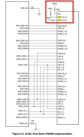
Using 2x LPDDR4 devices
We currently only support one LPDDR4 device. Trying to design with 2 LPDDR4 devices would require routing the data bus to two different devices, which we don't support.
The routing for dual rank would be the same as Fig 2-2 in the DDR layout appnote, with the addition of connecting CS1 and CKE1.
AM625: 16bit DDR4 performance
The AM62x app report has been out for a while, see memory bandwidth and latency sections in https://www.ti.com/lit/pdf/sprad45 .
AM625: DDR CLK termination specification
This is actually taken from the DDR4 recommendation from Micron, in their appnote TN-40-40. Here is the quote from the appnote:
If simulations determine that AC termination is needed, terminate CK_t and CK_c through approximately 36Ω series resistors and a .01uF capacitor to VDD. A single approximately 36Ω resistor in parallel across CK_t and CK_c may also be adequate
AM625: 2 DDR4 two, 4GByte total
According to the design of the EVB board, the 16-bit DDR is also not VTT added, which appears to conflict with what is mentioned in sprad06.pdf. Which should be referenced?
The EVM has only one DDR4 device, which only presents one load on addr/ctrl signals. Your design has 2 x8 devices and thus two loads, which would necessitate VTT termination because of the multiple loads. We are in the process of adding this detail to the app note. VTT-less design should only be used with one DDR device.
AM625: Supported DDR4 SDRAM Combinations
2x MT40A4G8 can be supported. Each device would be connected to each data byte. The address/ctrl signals would be connected in fly-by topology with VTT termination. I would recommend performing board level simulations to ensure proper signal integrity
AM625-Q1: Is it possible to change the drive strength on AM625-q1 for DDR lines.
for simulations, they have to change the model in order to choose a different driver setting. The driver strengths can also be change for silicon using the DDR register configuration tool: https://dev.ti.com/sysconfig/?product=Processor_DDR_Config&device=AM62x
AM625: external and internal spread spectrum oscillator support
AM625: LPDDR4 configuration and operating temperature
So, for example, if you plan to operate all the way to 125C, change the Operating Temperature Range to -40C to 125C. This also automatically de-rates some of the appropriate parameters (you can see these in the DDR datasheet) (this answers your last question)
You will also have to make the following changes manually in the tool
tREFIab = 975ns
tREFIpb = 122ns
tRASmax = 8775ns
tDQSCKmax = 3.6ns
Note that the next release of the DDR register configuration tool (post v9.08) will make these changes automatically when you change Operating Temperature Range. Once the SDK support dynamic changes, the config tool will change accordingly.
AM623: Operating temperature range at DDR config
we are in a bit of a transitional period to help support the range of temps supported by DDR.
First for LPDDR4, i believe the v9.1 of the SDK (not released yet) will support dynamic changes (ie, temperature controlled refresh mode). Currently, you have to choose the highest temperature you plan to operate, and configure the DDR Register Configuration Tool for that temperature. The latest version of the tool v9.09 will automatically change the appropriate parameters when the temp setting is changed in the tool. You will see these values change in the tool as you change the temp setting. Since dynamic refresh rate changes aren't support yet, the tool will simply configure the refresh rate to 4x to support the higher temps. It will also derate some of the other timings automatically, so all you should need to do is set the temp in the tool appropriately (there appears to be some typos in the README related to this, which will get fixed in the next release)
For DDR4, it is a different story. DDR4 doesn't have the same temp refresh mode as LPDDR4, so this is not relevant for software to support. In the tool, you would choose the appropriate temp range for your design, and this will change MR2[7:6]= 11b to support auto self refresh mode. MR4[3:2] will also be changed to 11b to support temperature controlled refresh. tREFI, tRFC, and tRAS do not automatically change, so this will need to be done by the user. A future version of the tool will auto change the refresh rate to facilitate this.
AM625-Q1: When using the AM625, executing commands may cause system crashes.
we identified that they're actually use a 512MB ddr4l memory on board but not configure the uboot and kernel memory size correctly within both sites of dts, to reflect 512MB judge from the logs they provided and customer's schematic design.
To configure DDR size in U-Boot, it is in the same memory@800000000 node, but in U-Boot file dts/upstream/src/arm64/ti/k3-am625-sk.dts.
Specifically for 512MB DDR, you would also need to add
CONFIG_SYS_MEM_TOP_HIDE=0x02500000
to U-Boot file configs/am62x_evm_r5_defconfig and cofigs/am62x_evm_a53_defconfig.
Miscellaneous
The processor conforms to the JEDEC LPDDR4 spec, so you should be able to get the information you are looking for from that spec.
The AM62x is JEDEC compatible to the LPDDR4 spec.
Kindly let us know the JEDEC standard number your referring to. We need this information to cross verify with the lpddr4 part.
it is LPDDR4 JESD209-4B
Can we perform Signal integrity validation check on the DDR clock probed on the vias without causing any loading effect due to the probe.? kindly let us know.
Yes, typically you would need to use high speed active FET probes
Would it be possible to monitor the lpddr4 signals through JTAG? Can the lpddr clock frequency be measured through JTAG? Can the lpddr4 timing parameters like setup,holdtime be validated through JTAG? We have the XDS110 JTAG debugger from TI .pls let us know if we can use this debugger to monitor the lpddr4 signals.
No, JTAG is just used for debugging code or in some instances for code trace capabilities. There is no way to measure signals using JTAG.
[FAQ] AM623: LPDDR4 Padstack size
PCB pad is NSMD and LPDDR4 package pad is SMD, so the PCB pad should be smaller than the Ø0.40 SMD opening on LPDDR4 package. The ratio is 1:0.8 (Pkg SMO: PCB pad)
With NSMD, the pad can be smaller as solder wets the sides/wall of the pad.
Note that the raw ball size is Ø0.436mm according to Micron datasheet.
Refer to https://www.micron.com/content/dam/micron/global/public/products/customer-service-note/csn33-bga-user-guide.pdf
* Table 3: Examples of Recommended PCB and Package Interconnect Opening Dimensions
* Printed Circuit Board Design Guidelines (pros and cons)
- NSMD pads are smaller and offer more space for trace routing than SMD pads
- SMD solder joints have higher standoff, which makes the joints more robust during shock or drop events
Consider Board Level Reliability Testing for your end product
Refer also to IPC publication 7351 Generic Requirements for Surface Mount Design and Land Patterns
You have to ensure to maintain only 1 load on each of the data bytes. You cannot connect devices in parallel where the data bus would be split on the board.
You can use something like Micron's MT40A4G8 and use 2 ranks to achieve up to 8GB, or you can use the single rank MT40A2G16 to achieve 4GB
Software patches to achieve 4GB can be found in this thread: https://e2e.ti.com/support/processors-group/processors/f/processors-forum/1235702/am623-memory-can-t-be-configured-to-4gb-from-device-tree/4681818#4681818
we don't have a tool for this type analysis at this time. I would suggest to perform high stress memory tests to prove out your board design. We typically use linux memtester at your max operating frequency, and across temperature if possible, to ensure a stable interface.
AM62x only supports DDR4 and LPDDR4 devices. Please refer to the datasheet for max frequency/size specifications.
You can refer to our SK-AM62 for a recommended DDR4 implementation using MT40A1G16KD-062E IT:E. This page should have all design documents which may simplify a customer design: https://www.ti.com/tool/SK-AM62
I would also recommend the customer review the DDR Board Design app note for any additional information on how to design a successful system: https://www.ti.com/lit/pdf/sprad06
The DDR4 I/O model is contained within the IBIS model for AM62x which is available on ti.com. No separate controller timing model is required for SI simulations.
ok this will occur during a power down sequence as show in figure 7-6 of the datasheet. Note that the first thing is MCU_PORz activating low, this will put the DDR subsystem in reset (and thus the DDR PHY) and tri-state all DDR signals. If they want to ensure CKE low, they would need a pull down on the signal.
I think the original question implied they were intending to keep the processor alive and just power down the LPDDR4, which i wouldn't recommend.
According to our experts, 50ohm DDR trace impedance will result in impedance mismatches in the system. The customer can design a board with 50ohm impedances, but they must run simulations for data read/write and addr/ctrl to ensure proper signal integrity.
the inline ECC feature should be available with any memory. I don't see a reason why it would not work. Note that i don't know the extent of software support for DDR ECC. It does take some configuration which i'm not sure is supported by the driver yet.
AM625: LPDDR4 configuration - how to configure IO configurations?
I helped the customer configure the timing parameters for this memory (attached syscfg).
However, I am unsure of how to configure the IO configurations and what they mean for the system and where to look for this info. Can you suggest me what the right configurations should be for this LPDDR4? In general, what resources should be followed to do this configuration?
IO configurations are usually taken from board simulations. Typically different values of drive strength and termination can be simulated to determine which setting provide the widest data eyes.
We need to understand if there is a valid procedure for first increasing the PMIC voltage (TPS651902 buck 1) and then boosting the A53SS to 1.4GHz post reset (during boot). You have not answered this question, and we require an answer so that the customer can move forward with their design.
AM62x doesn't support dynamic voltage scaling, so the PMIC can only be programmed to a fixed voltage to support AM62x.
I am not aware of the kind of DDR benchmarking you are asking about - we will have to see if the current thread assignee has any other input.
This discussion on another e2e thread about setting DDR access priority might be of interest to you:
https://e2e.ti.com/support/processors-group/processors/f/processors-forum/1220944/am625-lpddr4-access-priority
The M4F does have access to DDR memory, like the other cores. Please keep in mind that the M4F is different from the R5F cores, in that M4F does not have local cache memory. That means that each M4F access to data stored in DDR memory will take the full read time for the signal to travel out of the M4F, across the device, to the DDR, and back. At least on AM62x, we have measured M4F reads to DDR memory taking about 100 M4F clock cycles. Reference this FAQ for more information: https://e2e.ti.com/support/processors-group/processors/f/processors-forum/1187962/faq-sk-am62-how-to-execute-code-from-external-memory-using-m4f-core
Regards,
Sreenivasa
Hi Board designers,
Single rank LPDDR4 interface for AM62A, AM62D-Q1, AM62P
W66CP2NQQAFK is a single rank device, they should be referring to Figure 2-1 32-Bit, Single-Rank LPDDR4 Implementation in the app note. You can see from the diagram that address/control signals need to be T-branched on the board to connect to both channel A and B
Regards,
Sreenivasa
Hi Board designers,
Pins not supported on AM62L for DDR interface compared to AM62x
The DDRSS does not support DDR0_ALERT_n, DDR0_PAR, DDR0_CKE1, DDR0_CS1_n, DDR0_ODT1 signals (pins). It is recommended to follow the memory data sheet recommendations or consult memory supplier to connect any of the available signals that are not interfaced to the processor DDRSS
Regards,
Sreenivasa
Hi Board designers,
SK / EVM references for AM62L DDRSS interface
TMDS62LEVM AM62L evaluation module
https://www.ti.com/tool/TMDS62LEVM
The AM62L evaluation module currently supports LPDDR4 interface
SK-AM62B-P1 AM62x Starter Kit EVM with PMIC
https://www.ti.com/tool/SK-AM62B-P1
The SK supports DDR4
TMDS64EVM AM64x evaluation module for Sitara processors
https://www.ti.com/tool/TMDS64EVM
The EVM supports DDR4 with VTT terminations
SK-AM62-LP AM62x starter kit for low-power Sitara processors
https://www.ti.com/tool/SK-AM62-LP
The SK supports LPDDR4 interface
https://www.ti.com/tool/SK-AM64B
SK-AM64B AM64B starter kit for AM64x Sitara processors
The SK supports LPDDR4 interface
Note: AM62L DDRSS IP is similar with reduced addressable range.
Regards,
Sreenivasa
Hi Board designers,
Information related to DDR4connection of LDO VTTSNS
https://www.ti.com/lit/ds/symlink/tps51206.pdf
VTTSNS Connection

Figure 25. R-C Filter for VTTSNS
Regards,
Sreenivasa
Hi Board designers,
Information related to DDR4
I'm investigating a problem where some of our AM625 boards are not booting. One possible cause could be a problem with the DDR. Is there a tool, or similar, I can use to verify, or stress-test the DDR memory?
I'm aware that u-boot has such a feature but we cannot get as far as u-boot on these boards!
Please check the following page: https://e2e.ti.com/support/processors-group/processors/f/processors-forum/1358039/faq-board-bring-up-tips-for-sitara-devices-am64x-am243x-am62x-am62l-am62ax-am62d-q1-am62px
section "Running memtester (DDR memory test) from R5", this provides a patch that will run memtester immediately after DDR is initialized.
But before you do that, have you used the DDR register config tool https://dev.ti.com/sysconfig/?product=Processor_DDR_Config&device=AM62x to configure the DDR for your board? If you are using the default configuration from the SDK, you may need some tweaks to the configuration depending on the type of memory you are using or your board design (eg, configurations like drive strength and termination may need to be adjusted)
LPDDR4
DDR MARGIN TEST Tool
[FAQ] PROCESSOR-SDK-AM62X: Question about AM62x DDR MARGIN TEST Tool
Additional E2E and FAQs for reference
AM625: DDR Margin Tool
PROCESSOR-SDK-AM62X: DDR-MARGIN-FW for DDR4 SDRAM
Regards,
Sreenivasa
Hi Board designers,
Inputs related to DDR attached device reset pulldown.


What is the required tolerance for 10kohm resistor when considering PVT?
We don't spec a tolerance for that resistor. 10K was chosen because the previous resistor on our EVMs was 2.2K which proved to be too strong, and the Vih was sometimes not met for DDR_RESET_N.
If the tolerance of 10kohm is +/-10%, is it met for DDR_RESET_N?
yes +/-10% should be adequate
Additional inputs:
Please let me know the reason that 10kΩPD is OK in no circumstances(device PVT and variation of PD resistance value).
We can not know the drive strength of this I/O because there is no spec in datasheet.
This value has been shown in our characterization across PVT to provide a higher voltage level (vs using a 2.2Kohm resistor) when DDR_RESETn is deasserted during initialization. This provides better margin above Vih for that signal.
We would like the evidence that there is no VIH violation in no circumstances. Please let me know the minimum voltage level in worst condition with PD10KΩ. Or, please let me know the minimum drive level as VOH and IOH.
We don't specifically test this voltage level across PVT. The IO driver in this mode should be able to achieve VOH=>0.85*VDDQ and VOL=<0.15*VDDQ according to the IP vendor. They have checked this over PVT in simulation.
Regards,
Sreenivasa
Hi Board designers,
Inputs related to DDR design guidelines.
After reading this version of the DDR design guide www.ti.com/.../sprad66b.pdf, I have several confusions.
1. According to LP4_DRS6 in Table 2-7, the propagation delay of DQSx can be greater than DQ/DM.
However, in 3.5.3.2, 'DQSx delays must be less than the DQ and DM delays in the respective BYTEx' is mentioned. Which design rules should be followed?
2. Besides, is LP4_ACRS3 in Table 2-6 too strict compared to LP4_DRS4 in Table 2-7?
The package delay between DDR0_CK0 and DDR0_CK0_N has exceeded the value LP4_ACRS3. So I want to double confirm.
3. According to LP4_DRS3 in Table 2-7, does CK delay must be greater than DQS? Is 3*tck too loose?
1. Yes, the recommendation is that the DQS pair within a byte should have the shortest delay. As mentioned, the design allows for the DQ/DM to be shorter. We are adjusting the wording of the statement in 3.5.3.2 to align with the table
2. The skew on DQS and CK should be tightly matched as specified in the app note. I confirmed these differential pairs do have different skew requirements as noted in the app note (this was specified by the IP vendor). When performing skew matching, package delays should be accounted for. It is true that the package delay between CK0 and CK0_n is large, but it was recommended by the IP vendor to keep the mismatch in the package, and perform the length matching on the PCB.
3. Yes, CK delay should be greater than DQS to facilitate write leveling algorithm.
Is there is no additional skew requirement between DQs within bytes in table 2-7? We follow the 20ps skew between DQs , including the AM62D package. If there is no strict requirement, we can reduce many snake traces.
LP4_DRS5 in table 2-7 defines a max skew of 150ps. Where are you seeing 20ps?
20ps is the value we refer to some experience of PCB layout.
(+) AM62x: SK board DDR_VREFCA circuit - Processors forum - Processors - TI E2E support forums
On AM62x SK schematic Page 16, what is the purpose of C361 between DDR_VERFCA and VDD_DDR4, is it necessary or helps to stability DDR_VREFCA?

In app notes: AM64x/AM243x DDR Board Design and Layout Guidelines page 12, only mentioned to add 0.1uf near to VERFCA pin.
2.10 VREF Routing JEDEC defines two reference voltages that are used with DDR4 memory interfaces. These are VREFDQ and VREFCA. VREFDQ is the reference voltage used for the data group nets during reads and writes. VREFCA is the reference voltage used for command and address inputs to the SDRAMs. DDR4 SDRAMs generate their own VREFDQ internally. Similarly, the processor's DDR4 PHY generates its own VREFDQ internally. The VREFCA reference voltage must be generated on the board and propagated to all of the SDRAMs. VREFCA is intended to be 50% of the DDR4 power supply voltage and is typically generated with the DDR4 VTT power supply. It should be routed as a nominal 20-mil wide trace with 0.1-μF bypass capacitors near each device connection. Narrowing the VREF trace is allowed to accommodate routing congestion for short lengths near endpoints.
these caps help filter any noise from the DDR4 supply/ground (C361 and C363). The additional cap C362 is needed for decoupling near the VREFCA pin of the memory. .
Regards,
Sreenivasa
Hi Board designers,
Inputs related to DDR size:
Regarding the LPDDR4 connection, see
The [AM62x data sheet] (P1/263) states 4GBytes with LPDDR4, but the [AM62x, AM62Lx DDR Board Design and Layout Guidelines] (P22/44) states Max2GBytes. Which is correct?
[AM62x, AM62Lx DDR Board Design and Layout Guidelines] (P22/44) states that it is possible to connect the Dual specification with Single.
In this case, is it necessary to process the pins of the other memory area of LPDDR4?
it is technically possible to get 4GB of LPDDR4 with AM62x, however, as noted in the Layout guidelines, you would have to use a dual rank, dual channel LPDDR4 and only connect 1 rank to avoid splitting the data bus on the board. Thus, you would not be able to access half of the memory.
So the layout guidelines suggests that if you are needing more than 2GB of memory, you should use DDR4.
When using 4GB(Dual) of LPDDR4, do I need to process unused pins?
you can leave most of the unused pins unconnected. The unused DQS signals on the memory should be pulled to opposite polarity (ie, DQS_t pulled low, DQS_c pulled high) with a 1K resistor
Regards,
Sreenivasa
Hi Board designers,
FYI on connecting DDSS unused pins
AM62P: How to handle DDR pins required by only DDR4 when LPDDR4 is used?
My customer is drawing the schematic of AM62P.
They have question for DDR pins.
When using LPDDR4, how should they handle pins that are only used for DDR4? They checked the document "AM62Ax, AM62Px, AM62Dx LPDDR4 Board Design and Layout Guidelines" (SPRAD66B), but could not find the information.
Their understanding of unused pins when using LPDDR4
DDR0_a[13:6]
DDR0_ACT_N
DDR0_ALERT_N
DDR0_BA0/1
DDR0_BG0/1
DDR0_ODT0/1
DDR0_PAR
DDR0_WE_N
These signals can be left unconnected. Please refer the SK schematics implementation and follow the same.
Regards,
Sreenivasa
Hi Board designers,
FYI on simulations:
Could you please answer following questions?
Our customer is going to run SI simulation on SoC-DDR.
Could you tell us about the probe point when we simulate with IBIS model?
Which edge should customer use Die or Pad when at SoC side/Reads?
DDR4/LPDDR4 read simulations must show margin against the provided eye mask at the SoC DiePad. All other measurements are at the DRAM package pin as defined by the JEDEC spec.
DDR4/LPDDR4 uses both rising and falling edges of the DQS strobe during reads.
Refer to AM62x, AM62Lx DDR Board Design and Layout Guidelines https://www.ti.com/lit/an/sprad06c/sprad06c.pdf
4.5.3.3 Mask Report
The minimum jitter and noise margins are to be captured with respect to the eye masks. This masks are data
rate dependent, and includes:
• Data read eye mask at the SOC die pad for functionality testing.
• Data write eye mask (JEDEC spec) at the DRAM pin/BGA for compliance testing.
• CA bus eye mask (JEDEC spec) at the DRAM pin/BGA for compliance testing.
Table 4-3. LPDDR4 Eye Mask Definitions/Requirements
Read eye masks are defined here.
I added additional inputs from the simulation expert:
There is no concept of “probe point” while creating the IBIS model. It includes the package parasitics along with IO buffer details.
As regards their question about probe points for simulation, the customer should probe at the SoC die for DDR read simulations and Memory BGA (align with JEDEC) for DDR write simulations.
Regards,
Sreenivasa
Hi Board designers,
FYI on ODT configuration connection
TDA4VE-Q1: LPDDR4 design guide what the exact value for the pull up res of ODT?
From below guide, I can see the resistor value for others, but there is missing the value of ODT_CA_A/B, do we have any recommend value? In EVM, we are using 10K, but I want to double check about this, is it the best value? because from the Sitara AM62P board, we use 2.2K, and some customer is using 1K, so I want to figure it out, what is the best value? can you share some standard (Memory datasheet or JEDC?) customer need to follow, or any pull up resistor value can be accepted?
Jacinto 7 LPDDR4 Board Design and Layout Guidelines (Rev. F)
The specific resistor value is not critical - as its not a calibration or termination resistor value. It is a logic input - so any resistor value can be used as long as it sets the correct logic value. All the resistor values you mentioned (10K, 2.2K, 1K) should all be fine.
So if this signal is connected to 1.1v, the pull up resistor value is not matter, right? but previously in TDA4VEN EVM, customer connect to 0.55v(pull up to 1.1v with 10K and pull down with 10K), the DDR will have some stability issue (can work in low frequency, but failed in high frequency), and Micron lpddr4 can work in all frequecy, but Samsung and other ddr vendor can't work. this is interesting result if this is just logic input. capture from the micron ddr datasheet, can it be applied to all DDR vendor?
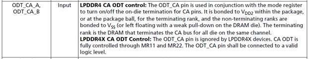
The signal is an input and the responsibility of the board design is to provide the proper logic high or logic low value. The mentioned 0.55V was an error because that is an invalid logic level. That voltage resulted from an on-board pull-up and on-board pull-down....which is a manufacturing mistake and not a valid implementation. There should be no pull-down resistor on board.
The 'weak' internal pull-down resistor and/or leakage current into the input pin may vary across memory manufacturers - so I recommended customer references those datasheets. (For example - in datasheet I am reviewing, I see no definition of weak internal pull-down, but I do see max input leakage of 4uA). In general - resistors in range of 1K to 10K should have no issue setting proper logic level for this pin.
Regards,
Sreenivasa