


Other Parts Discussed in Thread: TINA-TI, , OPA855
Hello,
My goal is to design a transimpedance amplifier that meets the following requirements:
- >= 1GHz -3dB cutoff
- (Ideally as high as 4-5GHz)
- >=+60dB gain
- Order of millivolts output swing to be fed into an ADC
I'm using currently using TINA-TI to simulate the TIA, with the ultimate goal of producing a tangible physical version of the circuit in the future.
The current source for the transimpedance amplifier will be coming from a theoretical HgCdTe infrared photodetector that outputs current on the order of magnitude of ones of microamps.
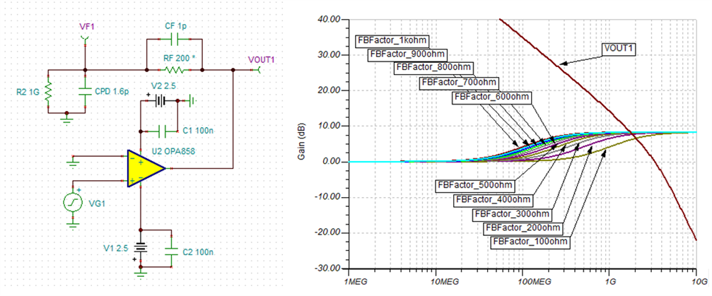
I have chosen to simulate the photodiode model as a shunt resistor of 1GOhm, AC current source of 1uA and frequency of 1GHz, and junction capacitor of 1.6pF in parallel, and currently have the OPA858 connected to that model in a negative feedback configuration. The OPA858 was chosen because of its 5.5GHz GBWP and FET-input (for ultra-low bias current).
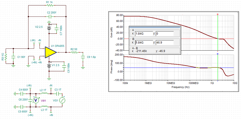
I'm fairly new to the world of amplifiers and their design considerations, and do not have a proper expectation of what my junction capacitance is going to be in the photodetector. For this reason, I've been playing around with the junction capacitance, feedback capacitance, and feedback resistance values to see how far I would be able to push the ability of a single OPA858. I don't know how to simulate a 50ohm BNC connection at the output somehow interfering with the circuit, so I just put a 50 ohm resistor and a capacitor to make a low pass filter that allowed 2 GHz through. Here is my current schematic and gain vs. frequency plot:

Right now, the only stable configuration I've been able to achieve is using CJ = 1.6pF, CF = 1pF, and RF = 200Ohm. I'm powering the OPA858 using a +2.5V and -2.5V power supply with 100nF decoupling capacitors in parallel with the battery. My criteria for stability was for the inverse feedback factor to be a relatively straight line when intersecting the open loop gain curve on a single graph, a technique which I learned from an AllAboutCircuits post.
I assumed that in general, as my feedback resistance increased my total bandwidth decreased, so I chose 200 ohms for the feedback resistance. This is in spite of the fact that my original goal was +60dB gain. At some point, I decided that I would leave the higher gain portion to a later voltage amplification stage that followed this transimpedance amplification stage, so I justified lowering the feedback resistance value here. I also worked under the assumption that, in general, sub-picofarad values for capacitors aren't feasible to work with in real life (the ultimate goal is to create the circuit), and that lower junction capacitance values yielded higher -3dB cutoffs, so I started with a junction capacitance of 1pF and worked my way up while trying to maximize the -3dB cutoff.
Here is the schematic and graph I used to choose the value of feedback resistor, holding the values of the feedback capacitor and junction capacitor constant at 1pF and 1.6pF respectively:
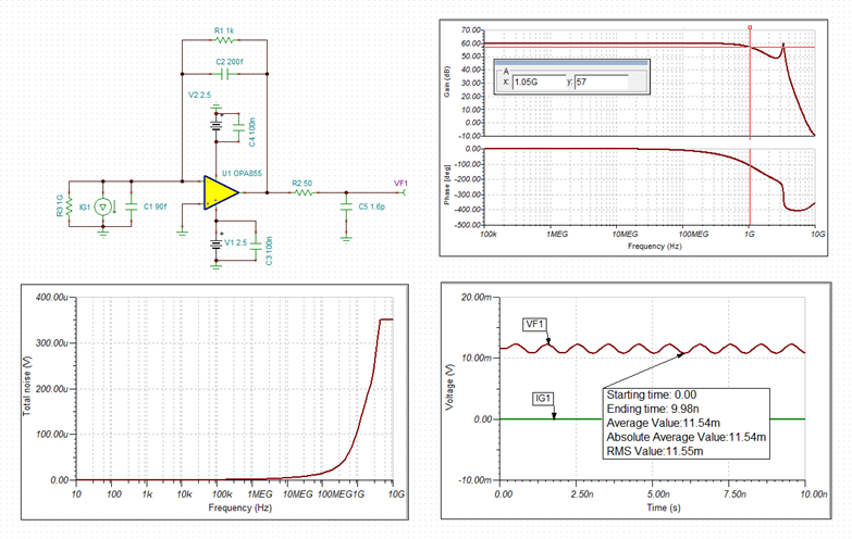
Although my signal to noise ratio will likely need to be much higher than a measly value of 1, a transient analysis of my graph from 0 to 10ns compared to the TINA-TI noise analysis function yields that noise overtakes the maximum value of my signal at 1.23GHz. Here are the graphs I used to come up with that information:

Which would lead me to believe that the uppermost limit of this circuit's bandwidth is 1.23GHz. But to add onto that issue, the phase graph produced by the AC transfer characteristic in TINA-TI is telling me that I pass -45 degrees at 410.31MHz, (of which I'm assuming based on some reading that the -45 degree mark is a value that helps to determine for what frequency range your circuit is still stable):
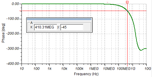
And so now, my circuit's "-3dB cutoff" has gone down from 1.68GHz to 410.31MHz.
There are a few major and minor problems I have with how I got to this point and future problems that I'm not sure how to think through, and for that I would request help:
- Problem 1: I don't know how realistic it is to even meet my design requirements. At the very least, I think I've come to the conclusion that it is impossible with just a single op-amp and no further circuitry.
- Problem 1a: I believe the junction capacitance of the actual photodetector that I would have available to use as the current source in this circuit would have a far higher junction capacitance than what I'm simulating (around 10nF), and I chose 1pF originally because I was just trying to see how much I could get from the OPA858. I don't know if (well, it probably is, but I don't know how to do it) it's possible to
achieve my design requirements knowing that the junction capacitance needs to be that high, and that the current output of the detector will be that low. - Problem 1b: The junction capacitance is a problem, but there also remains the problem of designing the system to be a working transimpedance amplifier that leads into a working voltage amplifier stage, and I don't know how to design a working voltage amplifier and how to couple the two stages together properly. Or if that's even the answer. I've toyed with the idea that having as much gain in a single stage will be the best option for minimizing my noise, so maybe the voltage amplifier isn't the right choice. I digress.
- Problem 1a: I believe the junction capacitance of the actual photodetector that I would have available to use as the current source in this circuit would have a far higher junction capacitance than what I'm simulating (around 10nF), and I chose 1pF originally because I was just trying to see how much I could get from the OPA858. I don't know if (well, it probably is, but I don't know how to do it) it's possible to
- Problem 2: I don't know how to properly evaluate signal to noise ratio in TINA-TI. My guess is that I should be using some metric like Vrms from the transient response divided by the "total noise" from the noise analysis function to acquire the SNR for any given frequency.
- Problem 2a: If I could reduce total noise while maintaining my signal amplitude, then theoretically that would also be a way of actually being able to use more of the -3dB bandwidth described by my original gain vs. frequency graph. I don't know how to reduce the total noise in this circuit.
- I've been trying to learn more about noise analysis and noise design considerations from the book "The Art of Electronics" and its supplementary material, the "X-Chapters", but I haven't been able to apply what it's been telling me to my design, from a lack of basic electrical engineering knowledge (confusing resistance/capacitance value choices, component choices, topology choices, too much focus on understanding solid state physics instead of getting the gist and moving on, etc).
- Problem 2a: If I could reduce total noise while maintaining my signal amplitude, then theoretically that would also be a way of actually being able to use more of the -3dB bandwidth described by my original gain vs. frequency graph. I don't know how to reduce the total noise in this circuit.
- Problem 3: I don't know how to increase the gain of this circuit while ALSO increasing the usable bandwidth of the circuit.
- Problem 3a: I've begun investigating a circuit topology called "bootstrapping" that supposedly allows transimpedance amplifiers to have higher bandwidth by reducing effective source capacitance by holding the AC voltage drop across the input capacitance low.
- I learned about this concept, along with the phrase "cascode" w.r.t transistor configurations that precede the "primary" op-amp in TIA circuits from Philip Hobbs' "Photodiode Frontends: The Real Story" and his book "Building Electro-optical Systems", but similarly to my approach with "The Art of Electronics", I'm just not fundamentally understanding how to apply the concepts he describes to my situation. That is:
- I learned about this concept, along with the phrase "cascode" w.r.t transistor configurations that precede the "primary" op-amp in TIA circuits from Philip Hobbs' "Photodiode Frontends: The Real Story" and his book "Building Electro-optical Systems", but similarly to my approach with "The Art of Electronics", I'm just not fundamentally understanding how to apply the concepts he describes to my situation. That is:
- Problem 3b: I don't know how to choose what op-amp or transistor I would use in a bootstrap configuration to actually achieve the higher bandwidth. I also don't know what value of coupling capacitor to use to tie the bootstrap amplifier in such a configuration together, or in general what a valid topology would look like for accomplishing my goal (is there also a negative feedback loop with feedback resistor and capacitor with the bootstrap amplifier? Should the output of that op-amp be attached to the same node of the photodiode model that's tied to ground? Should it even be an op-amp at all?).
- Problem 3a: I've begun investigating a circuit topology called "bootstrapping" that supposedly allows transimpedance amplifiers to have higher bandwidth by reducing effective source capacitance by holding the AC voltage drop across the input capacitance low.
Questions like these and more are currently sitting in my head while I'm also trying to properly digest the aforementioned reading material, never mind the fact that I've conveniently attached zero mathematical equations to back up any of the design choices I've made so far, largely because I have no confidence in any of the calculations I'd be capable of performing.
That is to say, I would appreciate any and all guidance and feedback with my problem, approach, and assumptions.
Thank you very much,
Gabe


 (example of SMA connector)