This thread has been locked.
If you have a related question, please click the "Ask a related question" button in the top right corner. The newly created question will be automatically linked to this question.
Hello,
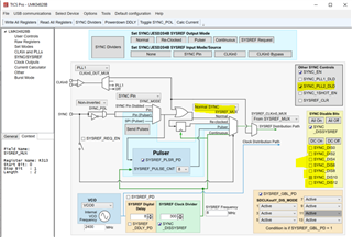
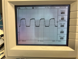
With the attached TICS Pro configuration, there is no SYSREF output from SDCLKout1.
Also attached is a copy of the schematic. LMK04828 circuitry is on Sheet 18.
Do I need to drive the SYNC pin (Pin 6) with a pulse or set it high?
Regards,
Andrew
Hi Andrew,
Sync requires a pulse or toggling SYNC_POL bit.
Procedure to setup SYSREF is found on page 40 of DS:
The EVM user guide also provides a quick example setting up SYSREF pulses using the default config:
Regards,
Vicente
Hi Vicente,
Is SYNC_POL bit the Pin 6 (SYNC)?
Can we also toggle once? Or do we need to pulse continuously?
And are there any timing requirements for the toggling or pulses?
Regards,
Andrew
Hi Vicente,
SYNC_POL is a register bit in 0x143.
Then I would need to do 3 register writes to toggle.
Could you clarify on the SYNC pin (Pin 6)? What is it intended for?
Thank you,
Andrew
Hi Andrew,
You're correct. SYNC_POL is a register bit.
You can also drive the SYNC pin using a pulse.
Performing a SYNC event can be done with either method.
Here is more on sync.
With SYNC_POL_INV = 1, the SYNC pin is active low.
Please let me know otherwise.
Let us try it.
Thank you so much
For clarification, SYNC_POL = 1 (for active low). Then I can drive the SYNC pin with an active low pulse.
Could you confirm if my understanding is correct?
Thanks again
To perform a sync via SPI,
Toggle SYNC_POL from L -> H and then from H -> L.
Regards,
Vicente
Hi Vicente,
0x000090 0x000010 0x000200 0x000306 0x0004D0 0x00055B 0x000600 0x000C51 0x000D04 0x01000F 0x010155 0x010255 0x010301 0x010422 0x010500 0x010670 0x010711 0x01080F 0x010955 0x010A55 0x010B00 0x010C22 0x010D00 0x010E70 0x010F11 0x01100F 0x011155 0x011255 0x011300 0x011422 0x011500 0x0116F0 0x011711 0x011818 0x011955 0x011A55 0x011B00 0x011C02 0x011D00 0x011EF1 0x011F11 0x012018 0x012155 0x012255 0x012300 0x012402 0x012500 0x0126F1 0x012711 0x012808 0x012955 0x012A55 0x012B00 0x012C02 0x012D00 0x012EF9 0x012F00 0x01300F 0x013155 0x013255 0x013300 0x013402 0x013500 0x0136F1 0x013706 0x013800 0x013900 0x013A01 0x013B2C 0x013C00 0x013D08 0x013E03 0x013F00 0x01400B 0x014101 0x014200 0x014319 0x014400 0x01457F 0x014600 0x01471A 0x014802 0x014942 0x014A02 0x014B16 0x014C00 0x014D00 0x014EC0 0x014F7F 0x015003 0x015102 0x015200 0x015300 0x015478 0x015500 0x015664 0x015700 0x015896 0x015900 0x015A64 0x015BD4 0x015C20 0x015D00 0x015E00 0x015F0B 0x016000 0x016101 0x016225 0x016300 0x016400 0x01650F 0x0171AA 0x017202 0x017C15 0x017D33 0x016600 0x016700 0x01680F 0x016959 0x016A20 0x016B00 0x016C00 0x016D00 0x016E13 0x017300 0x018200 0x018300 0x018400 0x018500 0x018800 0x018900 0x018A00 0x018B00 0x1FFD00 0x1FFE00 0x1FFF53 0x013900 0x014319 0x01000F 0x01080F 0x013A01 0x013B2C 0x014008 0x014319 0x013E03 0x014339 0x014319
After writing from 0x0000 thru 0x1FFF, I went thru the SYSREF setup process in Lines 137 and 147
0x013900
0x014319
0x01000F
0x01080F
0x013A01
0x013B2C
0x014008
0x014319
0x013E03
0x014339
0x014319
I may not have rewritten to the every recommended register but I think I addressed all the key steps.
I still don't seem to see the SYSREF output from SDCLKout1.
Could you take a look at the registers?
Thank you,
Andrew
Hi Andrew,
I opened up your config and see your VCO0 frequency is out of range:
The registers don't seem to add up with what TICs pro exports for this device.
can you double check this? If possible can you attach a .tcs file?
In regards to generating Sysref, it's important you follow all steps outlined.
Please note
Hi Vicente,
Here's the TICs pro file that generated the exported registers.
The VCO0 is 2400 MHz in TICs pro.
I'll also try again the SYSREF generation.
Thank you,
Andrew
Hi Vicente,
Would it be possible to receive a TICs pro file with Sysref running?
Or an example of exported hex file with Sysref generation?
I would just like to get an idea of how to correctly generate an Sysref signal.
Thank you,
Andrew
Hi Andrew,
With the above received config file (LMK04828b_v072123a.tcs), the device is in SYNC mode (SYSREF output is OFF) and all DCLK dividers will reset once the PLL2 is locked.
To generate the SYSREF in continuous mode, perform the below writes once PLL2 is locked.
1. 0x144 --> FF
2. 0x143 --> 11
3. 0x139 --> 03
Thanks!
Regards,
Ajeet Pal
Hi Ajeet,
In the screenshot you showed above, how should I change the check boxes?
The yellowed areas look the same as what I provided.
Thank you,
Andrew
The way we program the LMK04828 is
For completeness,
Thanks again!
In the meanwhile, I will try your suggestions.
Andrew
Hi Ajeet,
The 8-MHz Sysref is working after following your suggestions!
Also attached below are the .tcs (which is the same as yours) and the .hex file I used (basically exported from TICs Pro and added your suggested commands after 0x1FFF53
LMK04828_JESD204B_Config_Cust.tcs
0x000090 0x000010 0x000200 0x000306 0x0004D0 0x00055B 0x000600 0x000C51 0x000D04 0x01000F 0x010155 0x010255 0x010301 0x010422 0x010500 0x010670 0x010711 0x01080F 0x010955 0x010A55 0x010B00 0x010C22 0x010D00 0x010E70 0x010F66 0x01100F 0x011155 0x011255 0x011300 0x011402 0x011500 0x0116F0 0x011711 0x01180F 0x011955 0x011A55 0x011B00 0x011C02 0x011D00 0x011EF0 0x011F17 0x012018 0x012155 0x012255 0x012300 0x012402 0x012500 0x0126F1 0x012711 0x012808 0x012955 0x012A55 0x012B00 0x012C02 0x012D00 0x012EF9 0x012F00 0x01300F 0x013155 0x013255 0x013300 0x013402 0x013500 0x0136F1 0x013706 0x013805 0x013903 0x013A01 0x013B2C 0x013C00 0x013D08 0x013E03 0x013F00 0x014009 0x014101 0x014200 0x014311 0x0144FF 0x01457F 0x014600 0x01471A 0x014802 0x014942 0x014A02 0x014B16 0x014C00 0x014D00 0x014EC0 0x014F7F 0x015003 0x015102 0x015200 0x015300 0x015478 0x015500 0x015664 0x015700 0x015896 0x015900 0x015A64 0x015BD4 0x015C20 0x015D00 0x015E00 0x015F0B 0x016000 0x016101 0x016225 0x016300 0x016400 0x01650F 0x0171AA 0x017202 0x017C15 0x017D33 0x016600 0x016700 0x01680F 0x016959 0x016A20 0x016B00 0x016C00 0x016D00 0x016E13 0x017300 0x018200 0x018300 0x018400 0x018500 0x018800 0x018900 0x018A00 0x018B00 0x1FFD00 0x1FFE00 0x1FFF53 0x014400 0x014331 0x014311 0x0144FF 0x014311 0x013903
Thank you so much,
Andrew
ps: I would like to keep this for a few more days as I will now try to get the ADC working as well.
Regards,
Andrew
Hi Ajeet,
Could you review the schematic? I've also made notes on the clock related circuits.
Thanks again,
Andrew
Hi Andrew,
Glad to know, you are able to get the SYSREF outputs.
Regarding your schematic, please see below comments:
- DCLKOUT2p/n (ADCCLKP/N): On Slide 5, I think ADC32J25 is expecting LVDS. So should I update the resistors as noted in Slide 2?
- SDCLKOUT3p/n (SYSREFP/N): the same question here. Should I update the resistors?
From the ADC datasheet, below are the expected circuits for the LVDS and LVPECL input clocks.
Your board schematic, shows the termination for LVPECL input format. Hence, you can keep the R412, R415, R418 and R419 as it is and make the LMK04828 DCLKout2 and SDCLKout3 output setting for LVPECL format.
- DCLKOUT8p/n (PCIE_CLK1P/N): intended for PCIE. Please let me know if this looks appropriate
- SDCLKOUT9p/n (PCIE_CLK1P/N): intended for PCIE. Please let me know if this looks appropriate
Follow the section 10.4.2 of LMK04828 datasheet, if receiver doesn't have the internal termination, then can keep the 100ohm resistor across the DCLKoutx_P and DCLKoutx_N. Otherwise keep the 560ohm across them.
Based on PCIE receiver termination, you can follow the above suggestions.
Thanks!
Regards,
Ajeet Pal