Part Number: TDP1204
Tool/software:
Hey,
CMC Selections:
Please have a look at the CMC roadmap provided by Murata:
For any data rate above 12Gbps please use a common mode choke with sufficient bandwidth as to not attenuate the data signal.
ESD Selections:
We recommend the PUSB3FR4 for any data rate 10Gbps and lower.
When going above this data rate please look for an ESD with a lower capacitance and a clamping voltage between 3-4V.
-Vishesh Pithadiya
Part Number: DS125DF1610
Tool/software:
DS125DF1610 and DS110DF1610 are 16-channel retimers which implement 4x4 crosspoint switches.
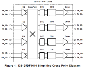
There are 2 registers which need to be configured to use the crosspoint: channel registers 0x96 and 0x9B.
Here is an example of a crosspoint configuration.
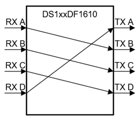
| Channel | Reg 0x96 Value | Reg 0x96 Comment | Reg 0x9B Value | Reg 0x9B Comment |
| A | 0x1F | Connects RX D to TX A | 0x01 | Connects RX A to TX B |
| B | 0x1C | Connects RX A to TX B | 0x02 | Connects RX B to TX C |
| C | 0x1D | Connects RX B to TX C | 0x03 | Connects RX C to TX D |
| D | 0x1E | Connects RX C to TX D | 0x00 | Connects RX D to TX A |
The DS125DF1610 and DS110DF1610 SigCon Architect GUI profiles have a bug on the Crosspoint Switch tab. Configurations made on this tab do not program register 0x9B correctly. Please verify low level register values are programmed correctly when configuring the crosspoint using the GUI.
Part Number: DS320PR810
Tool/software:
(Also applicable to DS320PR410, DS320PR1601, SN75LVPE5412, and SN75LVPE5421).
The datasheets for TI DS320PRxx and SN75LVPE5xx redrivers recommend the following sizes and numbers of power supply decoupling capacitors:
What purpose do each of these capacitors serve, and what is the best way to arrange or structure them?
Part Number: DS250DF230
Tool/software:
Across all 25-28G retimers (DS250DF210, DS250DF230, DS250DF410, DS250DF810, DS280DF810) there are 255 total CTLE boost settings. A subset of these settings, spanning the full range of the CTLE, makes up the CTLE boost table. Most 25-28G retimers use the same CTLE boost table, which includes 16 indexes spanning from 9.2 dB @ 13 GHz to 26.4 dB @ 13 GHz. DS250DF230 uses a unique CTLE boost table, which includes 20 indexes spanning from 0.6 dB @ 13 GHz to 26.4 dB @ 13 GHz.
CTLE Boost Table (DS250DF210, DS250DF410, DS250DF810, DS280DF810)
| EQ Table Index |
CTLE Boost Settings Reg_0x03[7:0] [Hex] |
High-Frequency Boost (10 MHz vs. 13 GHz) [dB] |
| 0 | 00 | 9.2 |
| 1 | 40 | 13.0 |
| 2 | 50 | 15.0 |
| 3 | 80 | 14.6 |
| 4 | 90 | 16.6 |
| 5 | C0 | 16.0 |
| 6 | D0 | 17.9 |
| 7 | D1 | 18.9 |
| 8 | D5 | 20.3 |
| 9 | D8 | 20.9 |
| 10 | EA | 23.5 |
| 11 | F7 | 23.8 |
| 12 | FD | 24.3 |
| 13 | EE | 24.5 |
| 14 | EF | 25.3 |
| 15 | FF | 26.4 |
CTLE Boost Table (DS250DF230 only)
| EQ Table Index |
CTLE Boost Settings Reg_0x03[7:0] [Hex] |
High-Frequency Boost (10 MHz vs. 13 GHz) [dB] |
| 0 | 00 | 0.6 |
| 1 | 01 | 2.0 |
| 2 | 02 | 3.2 |
| 3 | 03 | 5.4 |
| 4 | 00 | 9.2 |
| 5 | 40 | 13.0 |
| 6 | 50 | 15.0 |
| 7 | 80 | 14.6 |
| 8 | 90 | 16.6 |
| 9 | C0 | 16.0 |
| 10 | D0 | 17.9 |
| 11 | D1 | 18.9 |
| 12 | D5 | 20.3 |
| 13 | D8 | 20.9 |
| 14 | EA | 23.5 |
| 15 | F7 | 23.8 |
| 16 | FD | 24.3 |
| 17 | EE | 24.5 |
| 18 | EF | 25.3 |
| 19 | FF | 26.4 |
On the DS250DF230, the first three stages of the CTLE can be bypassed so that a very small amount of gain can be applied in the fourth stage only. This is why the DS250DF230 CTLE boost table includes 4 additional indexes and the minimum boost is much lower than other retimers. For short channel/low insertion loss use cases, DS250DF230 may be a better choice than other 25-28G retimers because of its minimum CTLE boost.
For all 25-28G retimers, the boost values for CTLE indexes 0-15 are programmed in channel registers 0x40 -- 0x4F, respectively. For DS250DF230, the boost values for CTLE indexes 16-19 are programmed in channel registers 0x50 -- 0x53, respectively. These registers are reserved for all other 25-28G retimers. TI strongly does not recommend making any changes to the boost values for each CTLE index.
If DS250DF230 is being configured through an external EEPROM, 4 bytes need to be included in the EEPROM hex file for registers 0x50 -- 0x53. These should be inserted between bytes which program channel registers 0x4F and 0x60. These 4 bytes are not included in the EEPROM hex file for all other 25-28G retimers.
EEPROM Register Map Excerpt (DS250DF210, DS250DF410, DS250DF810, DS280DF810)
| EEPROM Address Byte | Bit 7 | Bit 6 | Bit 5 | Bit 4 | Bit 3 | Bit 2 | Bit 1 | Bit 0 |
| 46 (0x2E) | 0x4E[7] | 0x4E[6] | 0x4E[5] | 0x4E[4] | 0x4E[3] | 0x4E[2] | 0x4E[1] | 0x4E[0] |
| 1 | 1 | 1 | 0 | 1 | 1 | 1 | 1 | |
| 47 (0x2F) | 0x4F[7] | 0x4F[6] | 0x4F[5] | 0x4F[4] | 0x4F[3] | 0x4F[2] | 0x4F[1] | 0x4F[0] |
| 1 | 1 | 1 | 1 | 1 | 1 | 1 | 1 | |
| 48 (0x30) | 0x60[7] | 0x60[6] | 0x60[5] | 0x60[4] | 0x60[3] | 0x60[2] | 0x60[1] | 0x60[0] |
| 0 | 0 | 0 | 0 | 0 | 0 | 0 | 0 | |
| 49 (0x31) | 0x61[7] | 0x61[6 | 0x61[5] | 0x61[4] | 0x61[3] | 0x61[2] | 0x61[1] | 0x61[0] |
| 0 | 0 | 0 | 0 | 0 | 0 | 0 | 0 |
EEPROM Register Map Excerpt (DS250DF230 only)
| EEPROM Address Byte | Bit 7 | Bit 6 | Bit 5 | Bit 4 | Bit 3 | Bit 2 | Bit 1 | Bit 0 |
| 46 (0x2E) | 0x4E[7] | 0x4E[6] | 0x4E[5] | 0x4E[4] | 0x4E[3] | 0x4E[2] | 0x4E[1] | 0x4E[0] |
| 1 | 1 | 1 | 0 | 1 | 0 | 1 | 0 | |
| 47 (0x2F) | 0x4F[7] | 0x4F[6] | 0x4F[5] | 0x4F[4] | 0x4F[3] | 0x4F[2] | 0x4F[1] | 0x4F[0] |
| 1 | 1 | 1 | 1 | 0 | 1 | 1 | 1 | |
| 48 (0x30) | 0x50[7] | 0x50[6] | 0x50[5] | 0x50[4] | 0x50[3] | 0x50[2] | 0x50[1] | 0x50[0] |
| 1 | 1 | 1 | 1 | 1 | 1 | 0 | 1 | |
| 49 (0x31) | 0x51[7] | 0x51[6] | 0x51[5] | 0x51[4] | 0x51[3] | 0x51[2] | 0x51[1] | 0x51[0] |
| 1 | 1 | 1 | 0 | 1 | 1 | 1 | 0 | |
| 50 (0x32) | 0x52[7] | 0x52[6] | 0x52[5] | 0x52[4] | 0x52[3] | 0x52[2] | 0x52[1] | 0x52[0] |
| 1 | 1 | 1 | 0 | 1 | 1 | 1 | 1 | |
| 51 (0x33) | 0x53[7] | 0x53[6] | 0x53[5] | 0x53[4] | 0x53[3] | 0x53[2] | 0x53[1] | 0x53[0] |
| 1 | 1 | 1 | 1 | 1 | 1 | 1 | 1 | |
| 52 (0x34) | 0x60[7] | 0x60[6] | 0x60[5] | 0x60[4] | 0x60[3] | 0x60[2] | 0x60[1] | 0x60[0] |
| 0 | 0 | 0 | 0 | 0 | 0 | 0 | 0 | |
| 53 (0x35) | 0x61[7] | 0x61[6 | 0x61[5] | 0x61[4] | 0x61[3] | 0x61[2] | 0x61[1] | 0x61[0] |
| 0 | 0 | 0 | 0 | 0 | 0 | 0 | 0 |
Part Number: DS320PR1601
Tool/software:
Do TI PCIe redrivers support bifurcation?
Part Number: TUSB1002A
Tool/software:
What is the purpose of the 330nF capacitors on the SuperSpeed RX and is it required?
Part Number: TCA9548A
Tool/software:
The TCA family of Texas Instruments I2C switches all support voltage translation. It's important to use the correct Vcc for the I2C switch to separate the voltages when channels are enabled. The only requirement is for the Vcc to be low enough to support this, as the Vcc voltage is the gate reference voltage for FETs inside the TCA switch/multiplexer devices.
Consider this scenario: the main SDA/SCL bus is pulled up to 3.3V, Ch1 is enabled with a pull-up of 1.8V, and the VCC of the device is 3.3V. In this scenario, with Ch1 enabled the VCC is too high in relation to the 1.8V pullup voltage, causing the drain-to-source impedance to decrease and turn on the transistor.
This creates a resistor divider between the two pull-up values. If these two resistors are the same, then the voltage on both SCL/SDA lines will likely be the midpoint of these two pull-up values. This midpoint voltage will be the voltage when the lines are idle.
Here's a simulation picture that makes this explanation clearer with both pull-up resistors being 5kΩ.
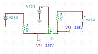
To avoid this error, designers must make sure to select the appropriate VCC for their device. The correct value can be found by referring to the Vpass diagram in the TCA datasheets. Vpass refers to the lowest pull-up voltage value on device channels, including the main SDA/SCL. For instance, if the lowest pull-up voltage is 1.8V on channel 1, this will be referred to as the passfet voltage, denoted as Vpass.
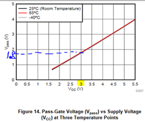
The maximum allowed Vcc is 3V for proper-level translation in applications where the lowest pull-up voltage is 1.8V. Designers should choose to use either 1.8V or 2.5V for the new Vcc, and the voltage translation of the TCA device will work properly with either option. Furthermore, a schematic demonstrating the voltage translation in action is provided below.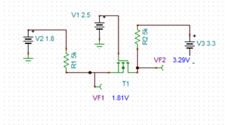
In summary, all the channels and the main SDA/SCL can operate at different voltages, as long as Vcc is within an acceptable range defined by the Vpass graph in the TCA datasheet. Vpass refers to the lowest pullup voltage connected to the TCA switch/multiplexer device.
Part Number: DS320PR1601
Tool/software:
Do TI PCIe redrivers require a PCIe Reference Clock (REFCLK) for operation?
Part Number: LMH1219
Tool/software:
Hi All,
It is common to wonder what is going on inside of ICs. Being an applications engineer at TI gives me the unique opportunity to report on this so that people can to understand our devices a little bit more.
In this E2E FAQ, I will be discussing a common pin configuration implementation that is used in our redrivers and in most if not all of our SDI retimers. 4-level input configuration pins have internal voltage thresholds to configure settings on the device. Some common settings that can be configured are ENSMB, OUT_CTRL, VOD_DE and many others.
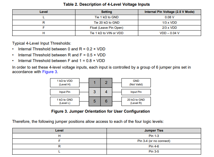
Using this excerpt from the LMH1219EVM user's guide, we can delve a little deeper into this topic. The four pin options are H,F,R and L, and they correspond to 4 different resistor configurations. If the pin was pulled low 1k ohms that would be L, if the pin was pulled 1k to VIN, that would be H, if the pin was pulled 20k ohms to GND, that would be R, and if the pin was left floating, that would be F.
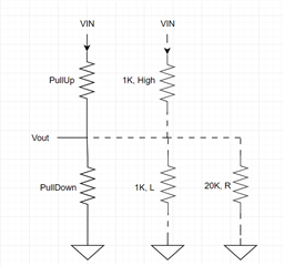
What a lot of customers do not realise is that typically this resistor ladder configuration includes an internal pullup resistor and pulldown resistor. These resistors effect Vout by ohm's law and the internal threshold values that eventually decide the device's operation are determined by the result of this resistor scheme. For example, for the LMH1219 the value for the pullup resistor is 30k ohms and the value of the pulldown resistor is 60k ohms.
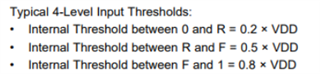
Say we have a 2.5V power supply. This means that the threshold between 0 and R would be 0.5 V and the threshold between R and F would be 1.25 V. As long as we fall between these two voltages, then the pin level will be R. When adding a 20 kΩ to ground, we can determine the voltage at the output based on adding a resistor in parallel with the 60 kΩ pull-down resistor, and this would give 0.83 V at Vout. By the same calculation with a 22 kΩ resistor, Vout would be approximately 0.87 V.
Best Regards,
Nick Peabody
HSSC Applications
Part Number: SN75LVPE5421
Tool/software:
First version of the data sheet required Cap to GND on RSVD pins 2 & 12. Then later revision called for zero-ohm Resistor to GND.
Whether we use 0-ohm resistor or Cap to GND this does not make a difference. SN75LVPE5412 schematic based on earlier version of the data sheet can continue using 0.1uF/0201 Cap to GND and this should not cause a problem.
Why was this done?
SN75LVPE5412 is pin compatible with DS160PR412. On DS160PR412 pins 2 and 12 are regulator pins and we required Cap to GND. In order for SN75LVPPE5412 to be pin compatible with DS160PR412, we recommended Cap to GND. In reality SN75LVPE5412 pins 2 & 12 can have either Cap to GND or tie to GND directly. If a customer wants to be pin compatible with DS160PR412 then we can use Cap to GND.
Regards, Nasser
