This thread has been locked.

If you have a related question, please click the "Ask a related question" button in the top right corner. The newly created question will be automatically linked to this question.

TLK10232EVM Question

Other Parts Discussed in Thread: TLK10232, CDCM6208

Hi.

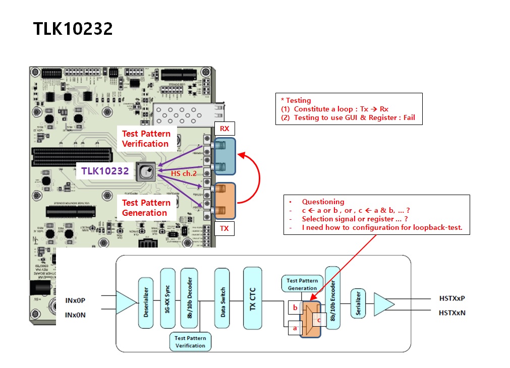
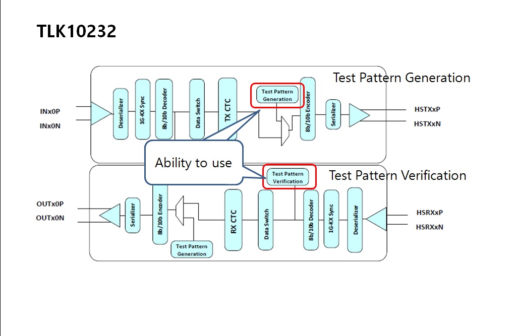
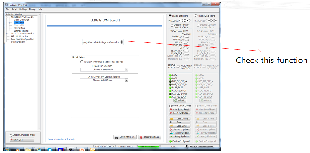
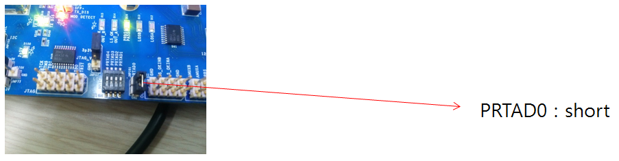
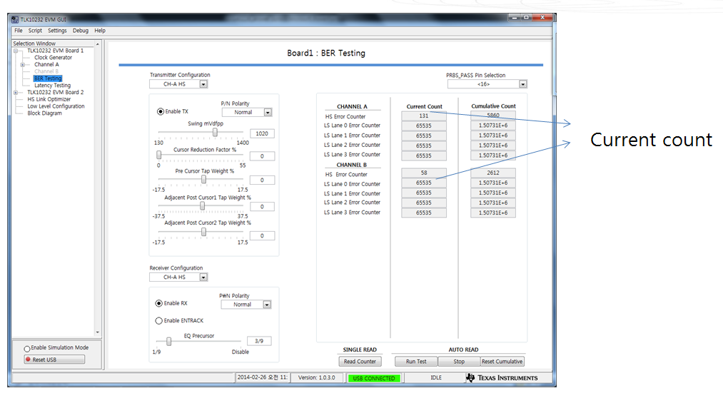
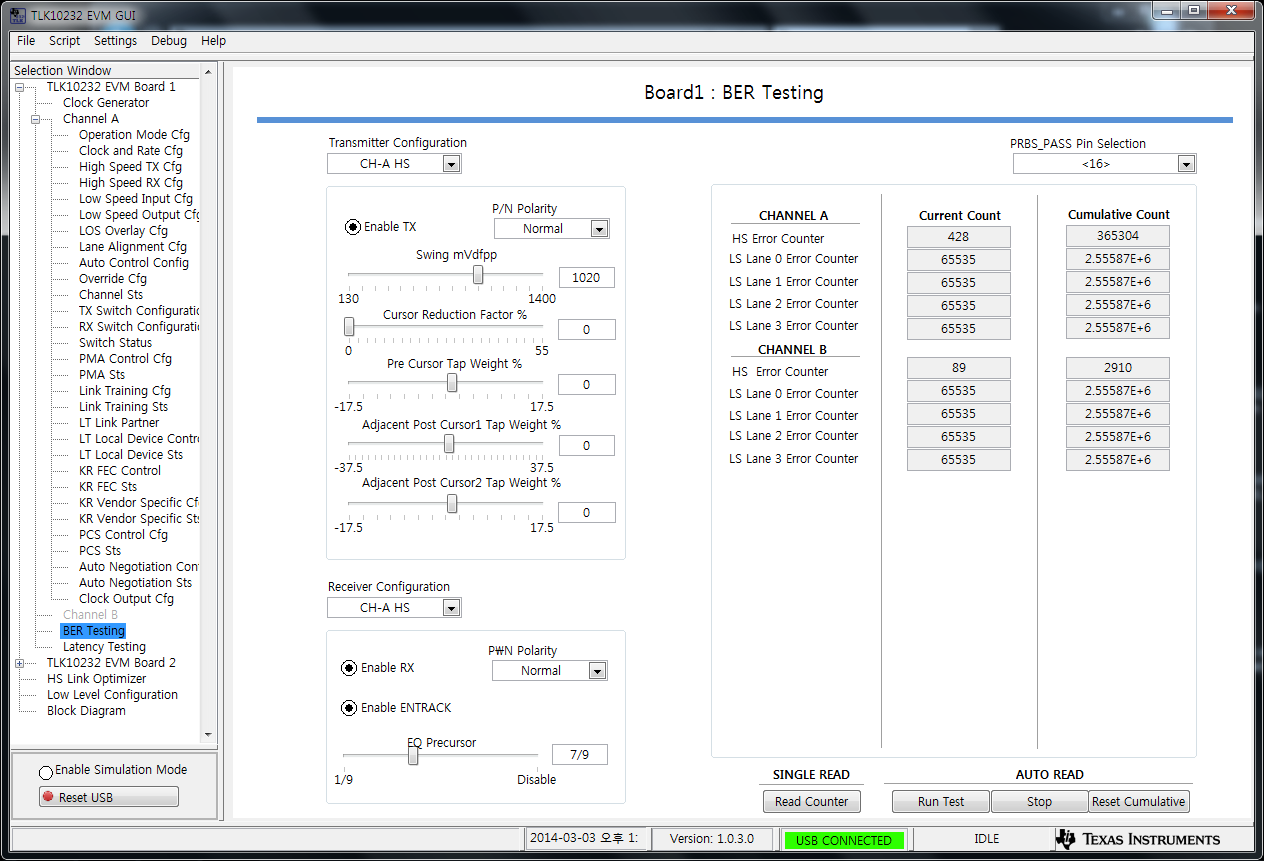
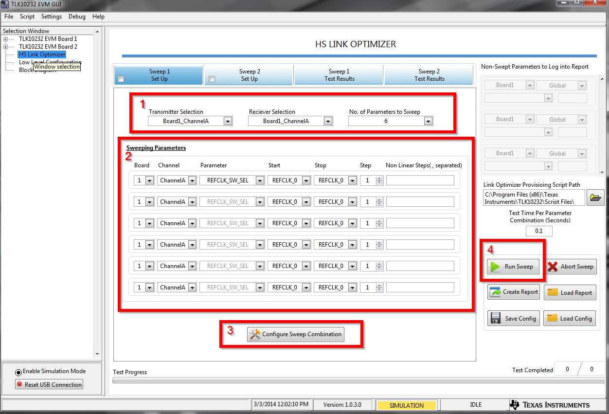
After power is applied to the EVB, (TEST Pattern (PRBS) Generation, TEST Pattern (PRBS) Generation function) BER tests on the steps (procedures) in sequence, tell us, testing in progress, which would help large.

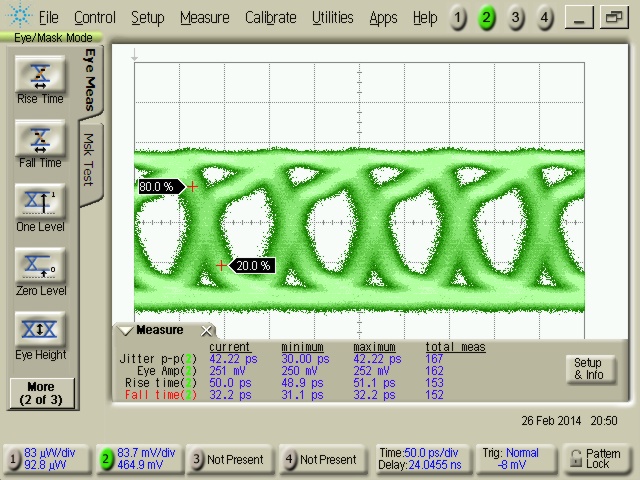
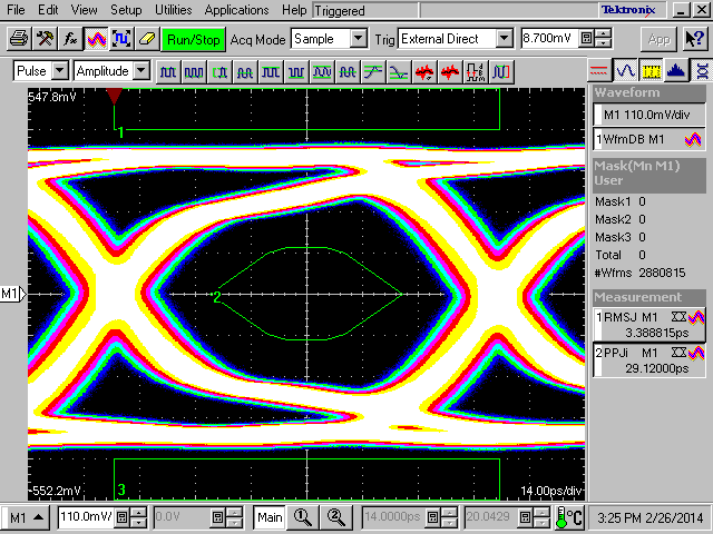
Test Pattern (PRBS) generation & verification test for the optical module functional electrical tests on the Loop, but this behavior has not been confirmed.
 
Documentation of test configurations and attached to the questions.

  • Hi Carl,

    A loopback BER test can be performed on either channel A or B. Channel A of the TLK10232 is mapped out to the SFP port on the EVM and channel B is mapped to the 4 SMA connectors that you have marked in your drawing. You simply have to connect the TX ports to the RX ports, it doesn't matter if you do A to, A to B, or B to B, then enable the test pattern generator and verifier with the desired test pattern. Once this is configure you can use the built in BER tester in the GUI to perform you BER test or you can go read the HS error register to see if errors are occurring or not. Hope this helps, please let me know if you have any more questions?

    Regards,

    Michael Peffers

    Analog Applications Engineer

  • Hi, Michael

    This is Matthew.

    Thanks for your answer.

    unfortunately, I can not see any pattern signal  on either channel A and B.

    II am trying see pattern signal of TLK10232 through OSC (Oscilloscope) or DCA (digital communication analyzer), but i can not .

    So, i'd like to solve this problem step by step.

    First of all, could you confirm a hardware config ? 

    8182.TLK10232 hardware config .pptx

  • Hi Matt,

    Can you effectively communicate with the EVM? When I work with this board in the lab the first thing I do is check that I can read and write one register from MDIO, I2C, and SPI. If you click Reset USB (lower left) and main board reset (right side) at different time on the GUI interface do you see the LEDs on the EVM toggle? These are all indication that tell you that you communication bus is working properly from the PC to the EVM.

    I really did not have much time to dig into this today because of other pending issues but it is top on my list for tomorrow. Everything looks accurate at first glance in your hardware setup but I will look closer tomorrow. In the mean time attached is a configuration script that will enable the TLK10232 to put out a PRBS31 test pattern at 10G on the HS side and 2.5G on the LS side. To load it simply put it on the desk top, or somewhere convenient to get to, and click load config on the GUI interface. Select this file and click apply updates and this will configure the device according to the attached script. Let em know how it goes?

    1638.LS and HS TP EN PRBS31 156.25 RefClk.csv

    Regards,

    Michael Peffers

    Analog Application Engineer

  • Hi, Michael ,

    I did test using your config.

    I saw patten signal .

    First of all , hardware config  had a little problem ( plz see the attachement file page 1)

    I could see the patten signal through HSTXBp when i changed hardware config.

    also i could see PRBS patten signal when i use your config.

    But the PRBS patten signal have some problem ( plz see the attachment file) also i can not check BER_test.

    7462.20140225_TLK10232 config .pptx


  • Hi Matt,

    I noticed in your attached presentation (which was great by the way, people usually do not put that much effort into stuff) that the ST pin is pulled high. This pin need to be pulled low for a 10G mode. Good catch on the PRBSEN pin, that one definitely needs to be low.

    I do not understand your output eye on page three though? Where was this eye collected from and what was your methodology? The output clock is the right frequency for the mode that you are in whicjh is a good sign. Can you please power cycle the device and restart the GUI. The reconfigure the chip using my script and check the output eye on channel B again? If the results are still not favorable, go to the low level register stack and read register 0x0f. Are you receiving PLL lock on both the HS and LS PLLs? Do you have channel sync?

    Regards,

    Michael Peffers

    Analog Applications Engineer

  • Dear Michael ,

    Thanks for your answer.

    I will test again about verification of pattern signal.

    Attached file is current status.

    There are some answer and some question .

    example , i can check BER_test but there is error  in spite of using direct connection..

                     and can improve 10Gpbs electric eye pattern ??

    I will answer again after testing pattern test..

    8585.20140226_answer .pptx

    Best Regards,

    Matthew.


  • Hi Matt,

    The "Apply Channel A Settings to Channel B" enables the GUI to write the same register settings to both channel A and channel be during the IC configuration.

    PRTAD0 is not needed for port addressing, but can be used as a general purpose input pin to control the switching function or the stopwatch latency measurement. If these functions are not needed, PRTAD0 should be grounded on the application board.

    The PLLs being locked is a good thing and tells me we are just making a fundamental mistake. The output eye that you are reporting still does not make any sense to me. The BER test you are running seems a lot better than what you reported yesterday:

    Have you tried connecting both the P and N signals and running the BER? This may have a positive effective on the running BER. While running the BER test trying sliding the EQ Precursor bar around to see if the BER improves. Also, try enabling ENTRACK bit. When implementing a short link the ENTRACK bit enables an internal low pass filter that will add ISI to the signal which helps the receiver compensate the signal better. When adjusting these features mentioned above make sure that you have the appropriate channel selected for the test you are running.

    If this situation does not improve on its own my fear is that one or more of the AC coupling caps is cracked on the Rx lines which will result in these tricking bit errors. Sometime when boards leave the board house they will have cracked resistor and/or capacitors because the pick and place machines depth is off by a little bit. I have seen this issue before but I am not convinced yet that this is the issue.


    Please try my suggestions from above and let me know what happens. There is another register value we can read to check link status but the address escapes me right now, I will provide this to you tomorrow when I am back in the office if we do not make any good progrss tonight.

    Regards,

    Michael Peffers

    Analog Applications Engineer

  • Dear Michael ,


    Attached picture is electronic eye pattern i saw that through HSTXBp .

    Could you confirm about this eye pattern(10Gbps) ?

    Is it best ?


    And There are error when i implement ber_test still... PLL's poblem..???


    Best Regards,

    Matthew. 

  • Hi Matt,

    The bit time for a 10G signal is a 100pS so please measure this on your scope. It is hard for me to tell from the picture that you provided. 

    Using the same script I sent you I measured and recorded the following eye diagram today:

    This is a forced 10.3125Gbps data pattern with CL73 and CL72 disabled. What does the BER look like when you are running a BER test. Is the error counter saturated or is it more like a trickling error rate? Are you seeing the errors on both channel A and Channel B?

    Regards,

    Michael Peffers

    High Speed Interface Applications Engineer

  • Dear Michael,

    the error rate is like a tricking error such as below picture ..

    condition : To select enable entrack

                     To adjust EQ precursor

    But i can not solve this problem  even though I implemented according to the your advise....

    Could you check again ?

    Best regards,

    Matthew.


  • Hi Matt,


    Typically when I see an issue like this with an EVM I will adjust the ENTRACK and or EQ Precursor to achieve an error free link as the channel needs to be tuned accordingly. If you have performed this and are still unable to get a 0 BER than I suspect that the data path has been compromised.

    Do have the ability to check the integrity of AC coupling caps and the 0 ohm resistors on HSRXn-p and HSTXn-p on channel B to see if they are cracked or not soldered correctly? You are looking for C247, C249, R581, and R582 which are located right behind the edge launch SMA connectors on the top side of the EVM. Are your cables of good quality and are they tightened appropriately to ensure a good connection? I have seen poor and loose cables cause an unstable BER in the past.

    Are you aware that you can tune channel B as well by selecting the channel B HS transmitter and receiver from the drop down menu in the BER testing window. Have you tried tuning channel B yet? For channel A there is no AC coupling caps in the data path so simply tuning the data path via the EQ Precursor and or ENTRACK should clear the errors up. Do you see any improvement or degradation at all when tuning the equalizer settings?

    How are you clocking the device, from the on board CDCM6208 or from an external clock source?


    Another test you can run is a link optimizer test:

    Simply select the channel you wish to sweep over (1), the parameters to sweep (2), configure the sweep (3), and lastly run the sweep (4). This process will generate a BER heat map for your swept parameters. You should be able to narrow down what settings will work the best for that board by performing this test.

    If all of the things mentioned above fail to produce a good link you can ship me the EVM back and I will ship you a new EVM. I believe we should not have to do this though as all the EVMs are tested before they are ever shipped to a customer. Please let me know what happens.

    Regards,

    Michael Peffers

    High Speed Interface Applications Engineer

  • Dear Michael,


    Thanks for your reply.

    I will test again according to the your suggestion method.

    I already check data path but there are no problem. Ok , i will check again.

    anyway,

    Attached file is electronic eye pattern each operating mode.

    10_KR and Auto negotiation mode have abnormal eye pattern..

    (I used 10G(4 to 1) operating mode when i sent eye pattern at previous e_mail.  )

    which part have a problem ?

    7635.20140304_checking eye pattern .pptx

    Best Regards,

    Matthew.

  • Hi Matt,


    When you are in an CL73 and/or a CL72 mode the test pattern needs to be generated from the PCS layer of the device not the typical HS generators and verifiers that you are using. If you are using the typical test pattern the PCS layer interprets this as invalid decodes because it is looking for 64/66 bit encoded data which may be causing the distorted eye pattern. Sorry, I should have been clearer about this earlier.

    Disable the HS TP that you are using now and go to the PCS Control Cfg tab within the GUI and active either the TX/RX Test Pattern Generation or the PRBS31 Test Pattern Generation on TX/RX path. I think that this will fix the abnormal eye pattern that you are seeing.

    Regards,

    Michael Peffers

    High Speed Interface Applications Engineer

  • Dear Michael ,

    I  could solve the issue of  "Tx pattern "and "  using this config (1638.LS and HS TP EN PRBS31 156.25 RefClk) at  operating mode of 10G(4*1) .

    But I still have a problem of 10G_KR mode and auto negotiation mode .

    Could you send optimized config of 10G_KR and negotiation mode ?

    I did test according to the your advise. => see the attachment file. 4087.20140305_10G_KR eye pattern .pptx


    Best Regards,

    Matthew.


  • Hi Matt,


    I was able to reproduce your results on the bench in the lab today. If you want to view the quality of the 10G-KR eye on a scope you must put the device in a forced KR mode where CL73 and CL72 are disabled. When I disabled CL73 but not CL72 and I observed the waveform it was very similar to what you have shown. So, you can either disable CL72 from the high level in the Link Training Cfg tab in the GUI or you can go to the low level PMA/PMD/LT_TRAIN_CONTROL bot 1 and disable it on the fly after the device is already configured. If you do the later make sure you perform a datapath reset (write 0x0008 to 0x0E) to reset the link.

    Please let me know how it turns out?

    Regards,

    Michael Peffers

    High Speed Interface Applications

  • Dear Michael ,

    I  did implement test according to the your advise. So i got the normal eye pattern .( => see the attachmenet file)

    5140.20140306 10.312Gbps eye pattern without CL72 .pptx

    Thank for your helpful. 

    By the way ,

    We try to merge  the control GUI of TLK10232 with Our' system GUI . we should be know control command and initial sequence if we control TLK10232 using our Sytem GUI.

    Could i ask S/W library (command) and Initial sequence ?

    Best Regards,

    Matthew.