Part Number: DS80PCI102
Tool/software:
The receiver detection is part of the transmitter and it must correctly detect if there is a DC load impedance - 40 to 60-ohm or lower - is attached at the output of the transmitter.
A transmitter - while at high impedance - changes the common mode voltage on plus and negative lead to pulse a step voltage. Based on measuring the voltage rise time the device determines if a receiver is attached.
Once it detects there is a termination on its output, then it turns on termination on its RX pins - 40 to 60-ohm.
Please refer to PCI Express 2.0 Base specification - for further details related to voltage step change and other details:
Regards, Nasser
Part Number: ETHERNET-SW
Tool/software:
This Master FAQ lists serves as a point of reference to find all FAQs made by TI's Ethernet Team.
Part Number: DP83TG720S-Q1
Tool/software:
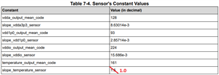
Section 7.3.1.4 of the datasheet outlines the procedure to use the inbuilt temperature sensor in the DP83TG720 PHY.
In order to maximize accuracy, please ensure the following:
Part Number: DP83867E
Tool/software:
For DP83867, and all RGMII PHYs within our portfolio, all pins marked with TX prefix (TX_D0-3, TX_EN, TX_CLK) are inputs to the PHY when operating in RGMII. The only timing specifications that are required for the input of the RGMII communication of PHY are setup and hold time, per datasheet. Rise and fall time are output characterizations of the PHY's RGMII transmitting signals (RX_DV, RX_D0-3, RX_ER, RX_CLK).
FAQ: Logic and Voltage Translation > IxC >> What I2C IO Expanders Support Automotive Grade 1?
There are a total of 3 to date.
TCAL9539-Q1 - 16-bit, 1.08V to 3.6V I2C IO Expander, single supply, interrupt, reset, Agile I/O Configuration
TCA6408A-Q1 - 8-bit 1.65V to 3.6V I2C IO Expander, dual supply, interrupt, reset, and config registers
TCA9539-Q1 - 16-bit, 1.65V to 3.6V I2C IO Expander, single supply, interrupt, reset, and config registers
FAQ: Logic and Voltage Translation > IxC >> I2C IO Expander Schematic Checklist
|
IO Expander Checklist |
|
|
|
Check |
Status (good, bad, okay, ?) |
Comment |
|
Local Decoupling Capacitors |
|
Generally, a 0.1-uF capacitor is placed on VCC, as close to the device as possible |
|
Verify the schematic pinout matches the data sheet pinout |
|
|
|
Check that the pullup resistors are present on the SDA and SCL net within the schematic. |
|
|
|
Unused GPIO pins are biased to either VCC or GND via resistor |
|
Most of TI's IO expander portfolio do not include internal pull-up resistors on the p-port pins; the exceptions are PCF8575, PCF8574, PCF8574A, TCA9555|PCA9555, PCA9554|TCA9554, and TCA9554A|PCA9554A and therefore can be left floating. An alternative approach is after powering up the device, any unused p-port pins can be set as an output (does not matter if set high or low). |
|
Device address is unique on the bus unless using an I2C switch or I2C MUX to resolve conflicts |
|
|
|
If the device has a /RESET pin, bias the pin high (preferably with a pull-up resistor) after powering up. |
|
|
|
If the device has a /INT pin and the /INT pin is used, tie this pin to a pull-up resistor. |
|
|
FAQ: Logic and Voltage Translation > IxC >> What is the Auto Increment Feature in I2C IO Expanders?
The auto-increment feature of I2C IO Expanders is when the registers of the device automatically increment to the next register in the set after consecutive writes / reads.
This feature is helpful if the IO expander is being written to or read from constantly. The constant writes and reads take up a lot of bandwidth in the I2C system. Auto incrementation helps to make the software more efficient which is especially helpful with heavily loaded I2C bus systems.
To understand this concept clearly, a picture of how to write a single byte to an I2C IO expander is shown below:
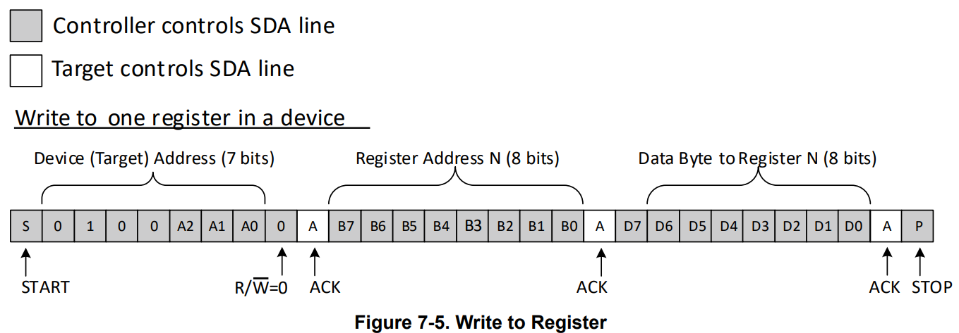
In the first byte, the device (target) 7 bit address is sent. Next is the "pointer" byte or register address. This is the register being written to. Finally, the third byte is the data to be set in the register selected.
In total, it takes 3 bytes of data to complete a single write transaction. For an 8-bit (8 IO) expander, this byte format is convenient since a single write can be utilized to change the state of 8 IO's at one time.
In the case that an IO expander has many GPIO's such as the 24-bit I2C IO expander TCA6424A. This same byte format would require 9 bytes of data in order to change all 24 IO's since it must write 8 bits at a time.
3 devices addresses, 3 register addresses, 3 data bytes for each register address
Auto incrementation removes the need to establish the pointer address every time a transaction is made. For example, if the user wants to write from all input port registers of the TCA6424A (Input port 0, Input port 1, Input port 2), the user can avoid rewriting the device address and the register address and simply continue the write transaction with the next data byte.
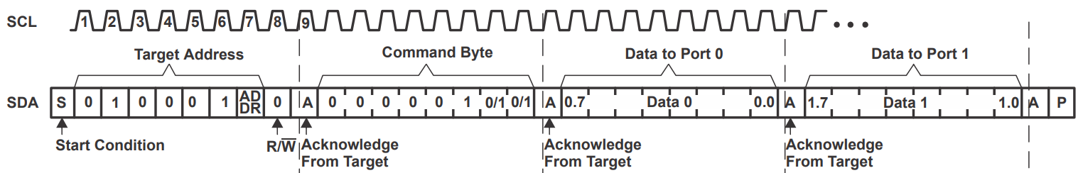
In this figure, the device address followed by the output port register address is sent. Data 0 is written to Output Port Register 0, Data 1 is written to Output Port Register 1, and so on.
Instead of writing 9 bytes of data to configure the 24 IO's, 5 bytes of data can be written.
1 x device address, 1 x output port register 0 address, 3 x data bytes = 5 bytes total.
For more information on the auto increment feature, please see the application note:
FAQ: Logic and Voltage Translation > IxC >> What is PassFET Hangtime?
To understand what passFET hangtime is, we need to define what a passFET is.
A passFET is a transistor where the drain and source terminals are interchangeable. The drain can be the source and the source can be the drain depending on the direction of communication.
This is especially import in I2C applications where bi-directional communication must occur for the protocol to work.
An example of a device that uses a passFET is the TCA39306 I3C/I2C capable level translator.
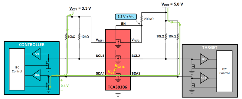
Controller pulling LOW through the TCA39306 level translator.
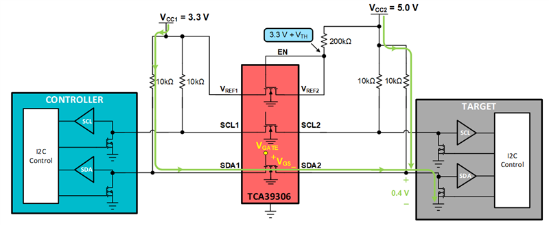
Target pulling LOW through the TCA39306 level translator.
PassFET hangtime is the time that the bus "hangs" during a high to low transition. PassFET hangtime occurs due to the parasitic capacitance on the I2C bus (CBUS1 & CBUS2). In the example below, the target pulls the bus LOW. It must first discharge the parasitic capacitance CBUS2 pulling the source of the passFET towards GND. Once the threshold voltage of the passFET between SDA1 and SDA2 has been surpassed the target sees the excess charge on CBUS1 in which the bus hangs.
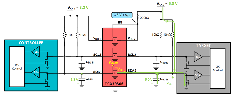
Target pulls LOW.
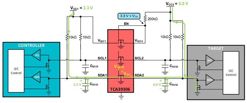
Target pulls LOW and begins to see the charge on CBUS1 in which the bus hangs for a time.
Below is an I2C address being sent.
CH1 = YELLOW = SDA1
CH2 = BLUE = SDA2
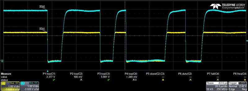
The effect of hang time is unnoticeable until the time scale is changed.
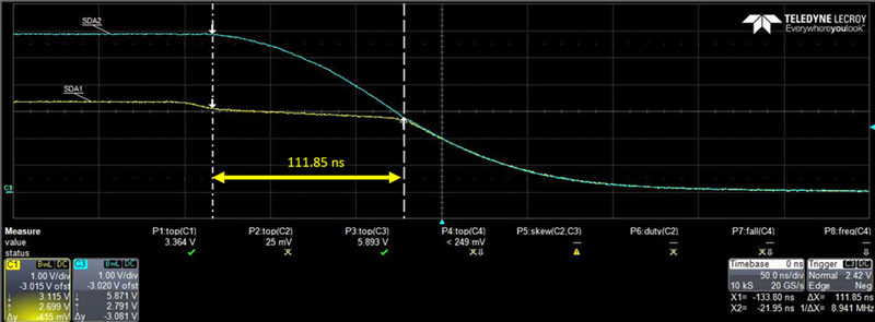
PassFET hangtime is measured to 111.85 ns in this example. Not enough time to make a significant impact on an I2C system, but the transition is there.
For more information on passFET hangtime, please see this application note.
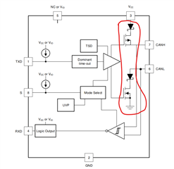
Part Number: TCAN1057A-Q1
Tool/software:
Hello experts!
I have a question about the purpose of the Mosfet and diode in CAN interface? Further,How does CAN implement arbitration and error correction functions through hardware?
Part Number: DP83822HF
Tool/software:
For DP83822, there is a guidance where AVD and VDDIO must not exceed 0.3V prior to complete supply ramp, with an additional footnote suggesting AVD to ramp up after VDDIO to avoid false detection of VDDIO. False detection may lead to non-operational performance from the device, such as no link up. If such a case is happening, it may be helpful to read register 0x421 to indicate what supply level the PHY is operating at and compare to intended levels. If a level is mis-detected, a way to bypass and rectify would be adjusting Reg 0x41F accordingly. Please note these registers are extended registers and thus will require 4-step process to read and write per datasheet.
