The following documents serve to provide recommendations for finding the right device to use in your system:
< Related Documentation>
[FAQ] What TI ESD/TVS diode should I use to protect Interfaces in my system?
Capacitance Requirements for High Speed Signals
< Related Threads>
Part Number: TUSB2E11
The eUSB2 interface is becoming increasingly common in designs with advance processors. In order to enable backwards compatibility with USB 2.0 hosts and devices, an eUSB2 repeater must be placed between the processor and the USB connector to convert 1.2V eUSB2 signaling to 3.3V USB 2.0 signaling. A common question from PCB layout engineers is where should the repeater be placed between the processor and connector?
Fortunately, the eUSB2 specification gives clear instructions on the maximum loss between the repeater and the processor, or SoC, as well as the loss between the repeater and the USB connector.
The max loss between the SoC and the repeater is -1.2dB, while the max loss between the USB connector and the repeater is 2.0dB. This translates to around 10 inches of loss between the repeater and SoC, which allows flexible placement in most designs. The trace distance on the USB-side of the repeater is even greater, around 16 inches; however, some factors can increase or decrease this distance, like board material or the number of vias in the signal path.
For more layout recommendations for eUSB2 repeaters, please read our eUSB2 Repeater Design Guide.
Part Number: SN75DPHY440SS
My customer asked about changing positive signal and negative signal.
(i.e. applying positive input to DA0N, negative input to DA0P, positive input to DA1N, negative signal to DA1P, and so on.)
Is it okay to use this device like this and Is this fully operational?
Is it okay to swap the lane as well?
Part Number: DS280DF810
A common question when using a signal conditioning device is can the device support a data rate that is lower than the target data rate.
The answer to this is device dependent, but there are several key criteria to look for depending on the device type. For redrivers, CTLE boost is the primary consideration. For retimers, there are a few additional considerations beyond just CTLE boost.
CTLE Boost
Continuous time linear equalizer, or CTLE, is a functional block within both redrivers and retimers. The CTLE boost curve is responsible for compensating for channel insertion loss in order to reduce ISI jitter. Typically when selecting a signal conditioning device, it's important to know how much channel loss it can compensate for. The CTLE boost is a good indicator of this. CTLE boost is a frequency dependent parameter. For example, DS160PR410 provides around 18 dB of boost at 8 GHz, but only around 7 dB of boost at 2.5 GHz. Because of this, it's important to consider the nyquist frequency of your intended application. Selecting a device supporting a much higher data rate than intended your application will generally mean that the device is not able to provide as much boost in your application compared to what is listed on the first page of the device data sheet.
CTLE boost curves or tables are often provided in device documentation. These can be used to better understand the compensation capability of a device across frequency.
Retimer Specific Considerations
A retimer is typically bound to more specific data rates than a redriver. This is because the clock and data recovery (CDR) functional block is limited to locking to a fixed range for rates. A typical CDR circuit will support a range of data rates, and several sub-rates of this range. For example, the DS280DF810 supports retiming the following data rates:
| Test Condition | Min | Max | Unit |
|---|---|---|---|
| Full Rate | 20.2 | 28.4 | Gbps |
| Half Rate | 10.1 | 14.2 | Gbps |
| Quarter Rate | 5.05 | 7.1 | Gbps |
However, it is also possible for the retimer to support additional data rates through a CDR bypass configuration. For example, the DS280DF810 can support 1.25 Gbps signaling through the CDR bypass configuration. Typically a retimer operating in CDR bypass can also provide CTLE boost, but digital filters such as DFE and FFE are bypassed.
An additional consideration when operating in CDR bypass mode is that some retimers have limited output amplitude control while operating in CDR bypass. This may be important to consider if using the retimer in an application where the output amplitude is critical for meeting a specification.
Part Number: TUSB8041A
1: Check power on reset sequence waveform for 3.3v ,1/1v and GRSTz pin and see if it meets hub power on reset sequence timing
2: Check voltage on USB_VBUS pin and see if the voltage is around 0.5v
3: Check if the crystal is oscillating after upstream port is connected to host
4: Do not enable SMBUSz with a pulldown unless a SMBUS host is used, otherwise the hub will hang waiting for configuration
5: Do not connect SDA/SCL to an on-board I2C bus unless it will be used
6: Do not leave blank EEPROMs connected to the hub if not used, the hub will enter a programming mode.
7: Please make sure the layout incorporates the thermal pad as shown in the datasheet.
8: If you still have issue, please submit E2E ticket with schematic to review
Part Number: TMUXHS4212
When and how do I place the AC coupling capacitors for the passive MUX?
Part Number: DS320PR810
Applicable to all TI PCIe redrivers for Gen 4:
And Gen 5 devices as well:
Intuitively, it may seem like there should be a connection between data rate and power consumption. In PCIe Gen 4, bits are transmitted at a rate of 16 GHz for example, and at Gen 5 this rate is doubled to 32 GHz. Even when the root complex and endpoint aren't intending to send any data to each other, the PCIe transmitters will constantly send idle bits to maintain the link. In integrated circuits, power consumption is often associated with the switching behavior of amplifiers, so it could appear that the power consumption would be higher at a data rate where the output amplifier must switch twice as frequently. However, TI redrivers use an architecture with a relatively constant current output at all times and the frequency of switching has little effect on the overall power draw. As such, the power consumption of a TI redriver given in its respective datasheet is applicable to all data rates that the device might be operating at.
Note that this constant power consumption is a characteristic of linear redrivers, which only boost signals using analog methods. Retimers, more complex ICs that have digital functions such as clock data recovery (CDR), are expected to have variable power consumption based on the data rate. Indeed, many PCIe endpoints have their own comprehensive CDR subsystems and experience the same effect. The heatsink of a network card operating at PCIe Gen 5 may feel hot to the touch, but only somewhat warm when running at Gen 4.
Part Number: TUSB8041A
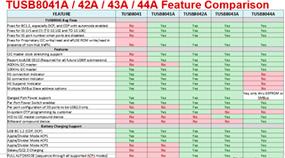
Over the time, TI TUSB804x USB3 hub family has been transitioned from USB3.0 to USB3.1, from TUSB8041 to TUSB8041A/8042A/8043A/8044A.
Here is the summary of major difference between these devices:
Functional Difference:
• TUSB8041 – USB 2.1 and USB 3.0 compliant, 4-port hub
• TUSB8041A – USB 2.1 and USB 3.1 generation 1 compliant, 4-port hub
• TUSB8042A – USB 2.1 and USB 3.1 generation 1 compliant, 4-port hub, with additional charging modes
• TUSB8043A – USB 2.1 and USB 3.1 generation 1 compliant, 4-port hub, with an HID programming interface and additional charging modes
• TUSB8044A– USB 2.1 and USB 3.1 generation 1 compliant, 4-port hub, with an HID programming interface, USB 2.0 Billboard support, and additional charging modes
• Default I 2C master bus speed: – TUSB8042A/43A/44A – I 2C master bus speed is 400 kHz
– TUSB8041 and TUSB8041A – I 2C master bus speed is 100 kHz
• USB 2.0 only ports: – TUSB8042A/43A/44A – Can report exposed USB ports as USB 2.0 only
– TUSB8041 and TUSB8041A – Feature not available, all exposed USB ports reported as USB 3.x
Major Feature Difference:
Part Number: TDP1204
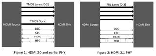
Brief Overview of HDMI PHY:
The HDMI physical layer is composed of 4 high-speed lanes, one Display Data Channel (DDC) which operates with I2C signaling, Hot Plug Detect (HPD) for device detection, Consumer Electronic Control (CEC), and HDMI Ethernet and Audio return Channel (HEAC). HEAC and CEC are both optional and do not affect video display.
For HDMI 2.0 and earlier versions the four high-speed lanes are defined as Transition Minimized Differential Signaling (TMDS) channels [0-2] and TMDS clock. For HDMI 2.1 the signaling changes to Finite Rate Lane (FRL). In HDMI2.1 the four high-speed lanes are defined as FRL lane [0-3], where the TMDS clock lane becomes FRL lane 3 and TMDS lane [0-2] becomes FRL lane [0-2].
The following diagram highlight the similarities and differences between previous HDMI versions and HDMI 2.1
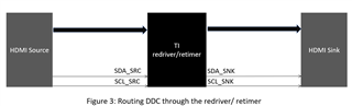
DDC Overview:
The DDC is used to control the status and configuration of the HDMI high-speed lanes. The signaling of the DDC is I2C, so the DDC is composed of the Serial Data (SDA) and Serial Clock (SCL) lanes. HDMI redrivers and retimers will have a SDA/SCL_SRC (source side connection), and a SDA/SCL_SNK (sink side connection). These are the pins that will be used for DDC snooping.
How to snoop HDMI:
There two are ways to route DDC when using a redriver/ retimer. Option 1 is routing through the redriver/ retimer and using the internal DDC buffer as seen in Figure 3.
Option 2 is to route the DDC lanes around the redriver/ retimer. In this case depending on the device pin definitions you need to connect the SDA and SCL line to the source side or sink side in order to snoop the DDC. This can be seen in Figure 4 and Figure 5.
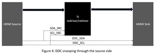
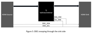
DDC snooping is used to correctly configure the redriver/ retimer to be in alignment with the source and sink. The snoop enable setting will be found in datasheet of the redriver/ retimer.
If the redriver/retimer is in pin strap mode, DDC snooping is necessary to set-up the device properly.
If the redriver/ retimer has an I2C mode, DDC snooping becomes optional as the configuration registers can be set manually using an I2C controller, or automatically using DDC snooping
