FAQ: Logic and Voltage Translation > Quality and Manufacturing >> Current FAQ
TI utilizes the Ultra Librarian software to provide symbols, footprints, and 3D models for our devices.
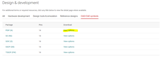
In the product folder for your selected device, scroll down and select "CAD/CAE Symbols" from the "Design & development" section.
Click the "View options" link that applies to the package you need:
This link will take you to the Ultra Librarian website:
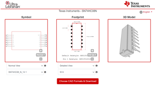
After selecting any options on this page, click "Choose CAD Formats & Download" to continue to the download page.
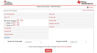
On this page you can select one or more formats for your download.
FAQ: Logic and Voltage Translation > Quality and Manufacturing >> Current FAQ
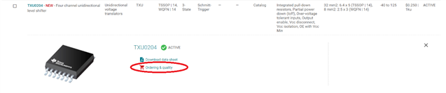
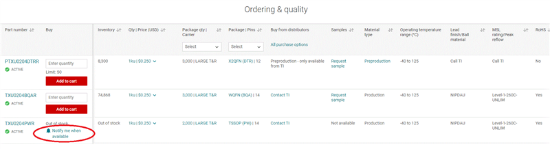
1. Search for the desired device in the TI store.
2. Click on the device and select the Ordering & Quality link.
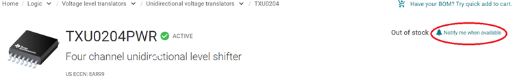
3. Select the Notify me when available link.
4. Select the Notify me when available link once more.
5. A pop up window will prompt you for the quantity and a valid email address. A pop up window should then confirm email notification is enabled
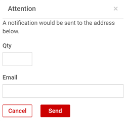
.
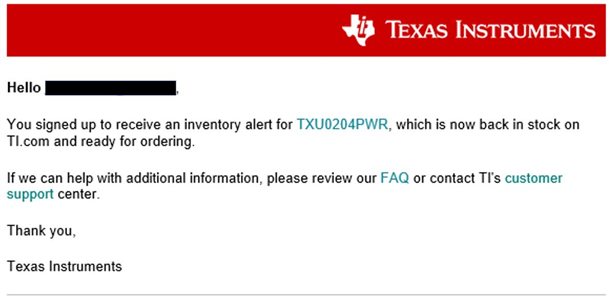
6. Once the device is back in stock you will receive an email notification as shown below
FAQ: Logic and Voltage Translation > Input Parameters >> Current FAQ
This question comes up fairly often because the HCS logic family is specified only at 2V, 4.5V, and 6V.
The following min / max values are interpolated from the datasheet tables, and thus are guaranteed by the datasheet specifications. Typical values are not guaranteed, however they are good estimates of performance under normal operating conditions.
HCS Family Electrical Characteristics
| PARAMETER | TEST CONDITIONS | VCC | MIN | TYP | MAX | UNIT | |
| VT+ | Positive switching threshold | 3.3 V | 1.22 | 1.93 | 2.36 | V | |
| VT- | Negative switching threshold | 3.3 V | 0.61 | 1.28 | 1.62 | V | |
| ΔVT | Hysteresis (VT+ - VT-) | 3.3 V | 0.3 | 0.65 | 1.21 | V | |
| VOH | High-level output voltage | IOH = -20 uA | 3.3 V | 3.2 | 3.298 | V | |
| IOH = -4 mA | 3.3 V | 3.14 | |||||
| VOL | Low-level output voltage | IOL = 20 uA | 3.3 V | 0.002 | 0.1 | V | |
| IOL = 4 mA | 3.3 V | 0.12 | |||||
| PARAMETER | VCC | MIN | TYP | MAX | UNIT | |
| fmax | Max switching frequency (HCS74) | 3.3 | 32 | 64 | MHz | |
| fmax | Max switching frequency (HCS165) | 3.3 | 83 | 91 | MHz | |
| fmax | Max switching frequency (HCS595) | 3.3 | 40 | 74 | MHz | |
Timing specifications are specific to each device -- please use linear interpolation for any timing parameters that need to be checked at 3.3V.
This related FAQ includes an Excel calculator to help speed this process:
FAQ: Logic and Voltage Translation > Power and Thermals >> Current FAQ
For the short answer - use a 0.1uF for single supply logic devices like the SN74LVC1G08, or a 0.022uF capacitor for each supply pin of a device with multiple supply pins, such as the SN74LVC16244A (which has 4 supply pins).
The purpose of a bypass capacitor is to provide a local supply of charge with very low impedance that can be quickly drawn upon by a component for power.
CMOS logic devices require significantly more power to be drawn during switching events than they do while in static operation, which means they must draw power quickly from the supply. Here's a plot of the expected current from a simple CMOS inverter during input switching events (simulated):
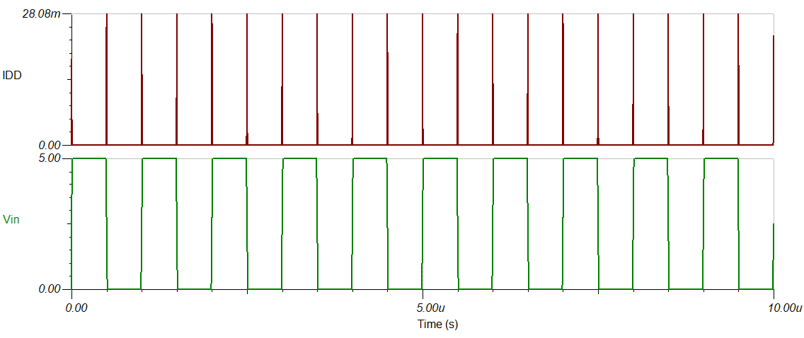
As you can see, there are short and sharp power spikes on each input transition. Because these current spikes are very short in duration and relatively large in value, having a local charge source is critical to provide consistent and reliable operation. Typically, a power supply will be electrically far from the logic device, which results in a relatively large inductance and resistance between the power source and the device's supply pin.
Additionally, these sharp spikes can cause power disturbances for other devices on the same power network. We want to prevent this, so bypass capacitors are added.
Bypass capacitors should always be placed as close as possible to the device, electrically speaking. This means that you want to have wide, short traces and have the capacitor physically close to the device. It can be placed on the opposite side of the board to reduce distance if desired.
In general, it's better to place the capacitor close to the supply pin and connect the other side to a ground plane through a via, then provide a via to the ground pin of the device as well. There are other methods that work, but this is the most common and easiest to implement.
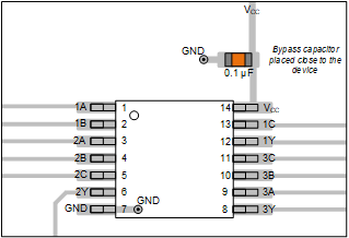
Example of bypass capacitor placement.
It's important to understand that capacitors are real components that include non-ideal behavior. This is a commonly used model for real-world capacitors:
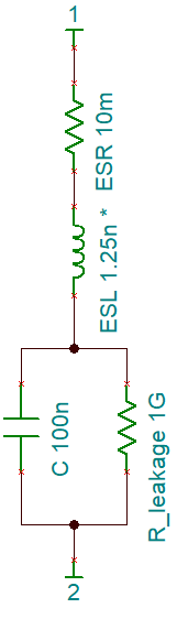
Of particular interest is the package inductance. If you recall the basics of inductors, they appear as open circuits at higher frequencies. This means that the capacitor will have an upper limit on the frequency range over which it can respond. Here's a plot of a capacitor's frequency response using typical values for a 0.1uF capacitor in a standard SMD package (1206).

* Note: This is not a plot for a particular capacitor, but a simulated response to show in general how capacitors respond.
The above plot is of gain vs frequency on a log-log scale (commonly called a Bode plot).The usable bandwidth for this capacitor ranges from approximately 100 kHz up to approximately 1 GHz (the "V" in the plot). At the lowest point, the capacitor has the lowest impedance, which is also the frequency at which it provides the most current (ie the fastest and best response). In this case, the capacitor provides the best performance just above 10 MHz.
* Note: The frequency plotted here is purely sinusoidal and relates directly to the edge rate of the logic signal - it is not related to the data rate or clock frequency of the signal.
-
By varying the capacitance and holding other aspects constant, we can see how the capacitor value affects the response frequency:
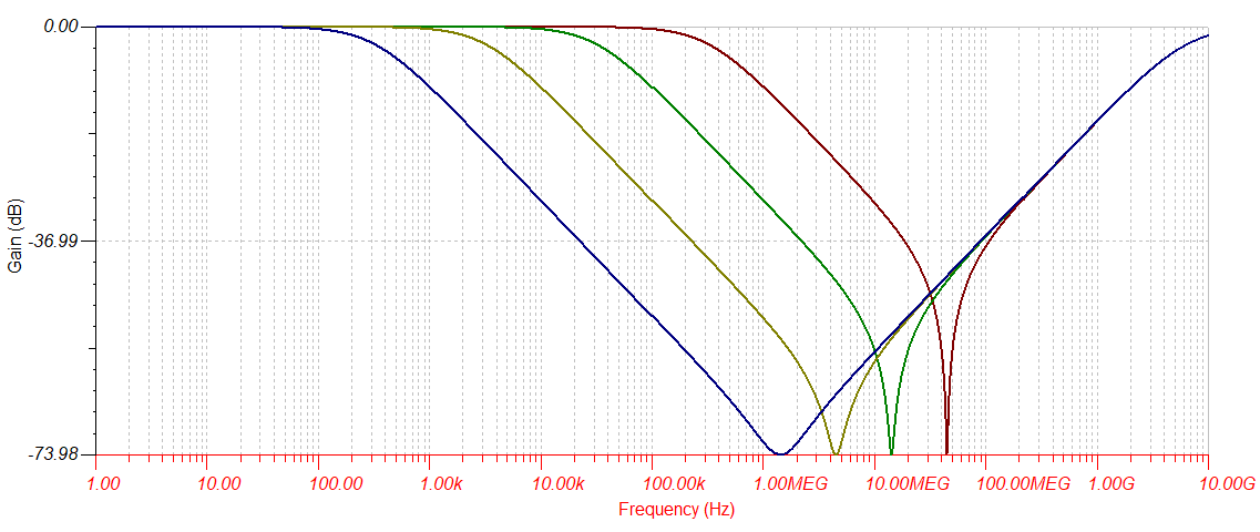
As the capacitor value is increased, the cutoff frequency on the low side decreases, while the cutoff on the high side remains constant. This is because the package inductance is being held constant while only the capacitance is changed.
-
If we vary the inductance instead by changing the package, we can see the opposite effect:
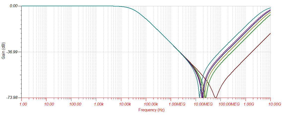
Reducing inductance by using a smaller package (or a package optimized for this application) will increase the corner frequency on the high-end of the plot, while the lower frequency will remain constant because the capacitance value is being held constant.
* I'm not going to go into a lot of details on capacitor performance for particular packages and types -- considering that I work for TI and we don't make capacitors, I think this is a discussion better suited for a capacitor manufacturer. If you're interested in this topic in detail, there are multiple app notes and articles available on the web that go into great detail regarding this and are quite interesting and informative to read. I won't be linking any of them because I don't want to appear to recommend a particular manufacturer -- sorry about that. Google is a great resource to find these -- you can start with searching for "choosing a bypass capacitor."
There are two primary criteria for selecting the best bypass capacitor value in a particular application:
1. Expected signal frequency components
2. Expected loading - including number of channels simultaneously switching
(1) For the first criteria, we have to look at the spectrum of a signal. I'm not going to go into a lot of details on this, but let's just say that an ideal logic signal (square wave) has infinite frequency components, but a real-world signal will have limited frequency components (search "ideal square wave bandwidth" for details). These are primarily controlled by the edge rate of the signal -- generally speaking, logic devices produce signals with primary frequency components up to around 300 MHz. Please don't confuse this with the operating frequency -- you can have a 1 kHz signal that has 300 MHz frequency components because the edges are very fast.
To ensure that you are able to source current as fast as necessary, the capacitor should have a bandwidth that includes as low of an impedance as possible at the desired maximum frequency. Generally speaking, a 0.1uF capacitor will cover a broad range of frequencies supporting from ~15 kHz to >1 GHz, however you can see from the above plots that it isn't optimized for a 300 MHz bandwidth signal. You could add additional parallel capacitors of smaller value to cover the higher frequency range. Here's an example using three capacitors in parallel of values 0.1uF, 0.01uF, and 1000pF:

(2) For the second criteria, we're looking specifically at how much charge is being drawn off of the capacitor with each switch of the output.
You can think of this in the context of charge sharing -- if you have a 0.1uF capacitive load on your logic gate, and you have a 0.1uF charge source for your power supply (with no other supply), then you would expect to get exactly half of the charge from your supply at the output, and thus your voltage at the output would be cut in half and half of the charge on your supply capacitor would be used up in the process.
Of course, the typical output load of a logic gate should be more like 10pF, so the charge sharing would be much different in a typical system. With a 10pF capacitor and 0.1uF bypass cap, the charge shared would result in 99.99% of Vcc at the output.
You wouldn't want to try to bypass the supply of a logic gate with only a 10pF capacitor, since that wouldn't be able to supply sufficient charge to the output. A a good rule of thumb is to keep your supply capacitor at least one order of magnitude larger than your output load. Again, a 0.1uF capacitor easily meets this criteria, so it's a good general purpose choice for a bypass capacitor.
FAQ: Logic and Voltage Translation > Output Parameters >> Current FAQ
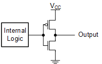
A push-pull output can source current in the high state or sink current in the low state. In modern CMOS devices, the most common configuration for a push-pull output is shown here:
|
Output State |
Positive Driver ( pFET ) |
Negative Driver ( nFET ) |
| HIGH | ON | OFF |
| LOW | OFF | ON |
When the output is in the high state:
The p-channel MOSFET is on and sources current from VCC to the output.
The n-channel MOSFET is off and does not allow current to flow to GND.
When the output is in the low state:
The p-channel MOSFET is off and does not allow current to flow from VCC.
The n-channel MOSFET is on and sinks current from the output to GND.
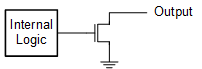
An open-drain output can only sink current in the low state. In modern CMOS devices, the most common configuration for an open-drain output is shown here:
|
Output State |
Negative Driver ( nFET ) |
| Hi-Z | OFF |
| LOW | ON |
When the output is in the high-impedance state, the n-channel MOSFET is off and does not allow any current to flow.
When the output is in the low state, the n-channel MOSFET is on and sinks current from the output to GND.
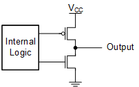
A 3-state output can be in one of three states: driving high, driving low, or not driving (high impedance). The most common configuration for a 3-state output is shown here:
|
Output State |
Positive Driver ( pFET ) |
Negative Driver ( nFET ) |
| HIGH | ON | OFF |
| LOW | OFF | ON |
| Hi-Z | OFF | OFF |
When the output is in the high state:
The p-channel MOSFET is on and sources current from VCC to the output.
The n-channel MOSFET is off and does not allow current to flow to GND.
When the output is in the low state:
The p-channel MOSFET is off and does not allow current to flow from VCC.
The n-channel MOSFET is on and sinks current from the output to GND.
When the output is in the high-impedance state:
The p-channel MOSFET is off and does not allow current to flow from VCC.
The n-channel MOSFET is off and does not allow current to flow to GND.
FAQ: Logic and Voltage Translation > Input Parameters >> Current FAQ
The short answer is - a floating node is a voltage node that is not being forced to a known voltage, thus it has an unknown voltage.
Some additional details follow:
In circuit theory, a voltage node refers to a shared connection that is at the same voltage. To illustrate, I have developed a simple circuit:

The red highlighted node in the above circuit can be referred to as a voltage node. The voltage across C1 and R2 is equal.
For my circuit analysis below I make two assumptions:
(1) R1 and R2 are much larger than 10 ohms
(2) A very long time has passed, allowing C1 to reach a steady-state voltage
With the circuit configured as drawn, with S1 closed and S2 open, the voltage at C1 is ~5V.
If S1 were opened and S2 were closed, the voltage on C1 would be ~0 V.
In the event that both S1 and S2 are open, this is called a floating node. The voltage on C1 is unknown because we don't know the precise values of R1 and R2 (these represent parasitics on the board - paths for leakage current).
Because this is an ideal circuit, we could set values for R1 and R2, and then solve for the voltage on C1 and the node voltage would be constant. In the real world things aren't that simple.
But what if we add a few more factors into the circuit? Let's assume R1 and R2 are huge -- in this case, 10 Mohm each. Let's also add mutual inductance, an additional resistive leakage path, and some parasitic capacitance to nearby active traces:

In this case, nearby voltages can influence the voltage of C1. Rather than staying at exactly 1/2 Vcc (due to the voltage divider with 2x 10 Mohm resistors), the voltage on C1 will likely slowly vary up or down. This is why the voltage is said to 'float' -- it can be easily influenced by nearby signals and leakage currents.
In real systems, this can get far more complex, with added inputs from numerous sources both on and off the board. Let's suffice it to say if you are not actively forcing a node to a known voltage, then it is a floating node and the voltage is unknown.
Eliminating floating nodes is important in CMOS circuits to prevent problems. You can see more about this here:
[FAQ] How does a slow or floating input affect a CMOS device?
Quickly find solutions to common questions about voltage translation (level shifter) devices by clicking this link. This FAQ answers the most common questions asked about these devices …… ……… …
| Auto-Bidirectional Level-Shifters | Fixed DIR / DIR CNTRL Level-Shifters | Ground-Level Translators | IxC | Generic | Use Cases & Part Recommendations |
Input Parameters:
Output Parameters:
Timing Parameters
Power and Thermals:
Quality and Manufacturing:
Simulation Models:
Monostable Multivibrators:
Logic Technology:
FAQ: Logic and Voltage Translation > Output Parameters >> Current FAQ
This question is really about the output structure of the logic device.
There are primarily two types of open-drain output structures - one with a positive clamping diode, and one without, shown here:

The positive clamp diode is shown in red. If the output voltage is higher than Vcc, then the positive clamp diode will become forward biased and will allow current to flow through to Vcc. This has two primary effects. First, it can provide power to the Vcc rail (this is an example of "back-powering" a device). Second, it's possible for the current through the clamp diode to become so large that it can permanently damage the device. This current limit is rated as "I_OK" in the datasheet, and is found in the absolute maximum ratings table. Here's an example of a device's abs max table with an input clamp diode
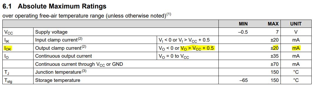
Note that the output clamp current can be turned on two different ways - going into the part (+20mA) and out of the part (-20mA) and there is a condition of V_O < 0 or V_O > Vcc + 0.5V. These are two indicators that there is a positive clamp diode. Here's an example abs max table for a device without a positive clamp diode:
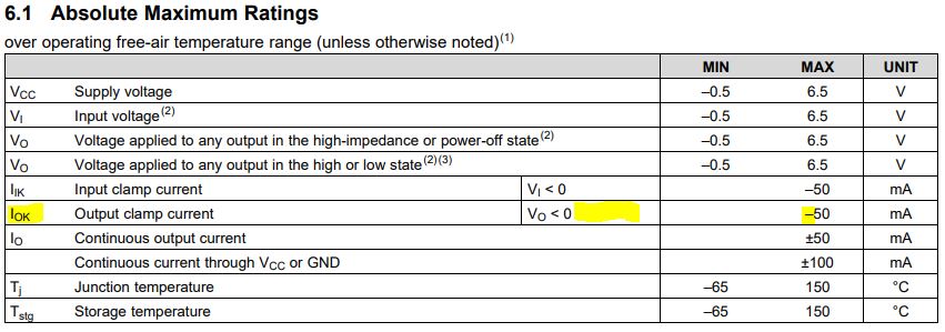
In this table, you can see that the positive current value and the condition of V_O > Vcc + 0.5V are both absent. This indicates that there is no positive clamp diode.
Another indicator is the maximum value on the output voltage. For a device with a clamp diode, the output voltage will be limited to Vcc or Vcc + 0.5V, however a device without the positive clamp diode will have a numerical value.
There is one more possibility for the output being a higher voltage than the supply, which is the case where the supply is off (Vcc = 0V) and the output is operating at some voltage higher than 0V. This case is covered partially by the above information, but also has a special feature associated with it called "Ioff - Partial Power Down Protection".
If a device is rated for operation with Vcc = 0V, the Electrical Characteristics table will include the value of Ioff, which is the leakage current into any input or output pin of the device when the supply is forced to 0V. Note that this spec is _only_ valid under the case that the supply is at 0V, and not just if the supply is disconnected (floating) or off (unknown voltage). Some supplies can still provide enough voltage to operate a device even though they are disabled -- for example, many boost converter circuits have a direct connection from the input voltage to the output through only a diode.
| Input Parameters | Output Parameters | |||
| Power and Thermals | Timing Parameters | Logic Technology | Quality and Manufacturing | Simulation Models |
